As the name implies, a zero-drift amplifier is an amplifier whose offset voltage drift is very close to zero. It uses auto-zero or chopping techniques (or both) and continuously self-corrects DC errors over time and temperature. This allows the amplifier to achieve μV-level offset and very low offset drift. Therefore, it is especially suitable for signal conditioning circuits with high gain and high precision performance. For example, sensors (such as temperature, pressure, or load cells) typically produce a low-level output voltage, so an amplifier is needed to amplify the signal and should not introduce more errors. Designed for ultra-low offset voltage and drift, high common-mode rejection, high power supply rejection, and lower 1/f noise, the zero-drift amplifier is ideal for high resolution in demanding system applications such as inspection applications. Has a long product life cycle.
Basic architecture of zero-drift amplifier
Figure 1 shows a circuit diagram of a basic chopper amplifier (unit gain configuration). The DC gain path includes an input chopping switch network (CHOPIN), a first transconductance amplifier (Gm1), an output chopping switch network (CHOPOUT), a second transconductance amplifier (Gm2), and frequency compensation capacitors (C1 and C2). CHOP and CHOP' are controlled by a clock generator and function to correct unwanted amplifier dc offset voltage (VOS).
Figure 2 shows the associated timing diagram and the expected output voltage (VOUT). When the CHOP clock signal is high (stage A), the differential inputs and outputs of amplifier Gm1 are connected to the signal path and are not inverted. The positive output voltage VOUT is generated due to the presence of VOS. When the CHOP' clock signal is high (B stage), the input and output of Gm1 are connected to the signal path and inverted, and a negative output voltage is generated due to VOS. The positive and negative output voltages from Gm1 make the output voltage equal to ±VOS. This chopping concept in the time domain is similar to modulation in the frequency domain. In other words, the Gm1 offset voltage is modulated up by CHOPOUT to the chopping frequency. On the other hand, the input signal is chopped twice via CHOPIN and CHOPOUT. This is equal to the input signal that is modulated up and then modulated down to the original frequency. Therefore, the input signal entering the output does not reverse.
The positive and negative output voltages (±VOS from Gm1) appear in VOUT in the form of voltage ripple (Figure 2). In addition, the CHOP and CHOP' clocks are coupled to the differential input pins via switch-related parasitic capacitance. After the clock changes state, charge is injected into the differential input pin. These injected charges are converted to output voltage spurs via a finite input source impedance. The magnitude and shape of the glitch depends on the input source impedance and the amount and matching of the injected charge on the differential input pins. These output ripples and spurs create switching artifacts that grow at the chopping frequency in the noise spectrum and at their integer multiples. In addition, the switching artifacts of each zero-drift amplifier vary in amplitude and frequency, and vary from component to component. In this document, the terms "chopper" and "switching frequency" are used interchangeably.
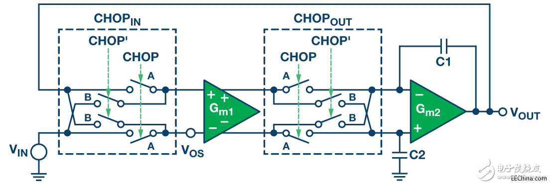
Figure 1. Chopping architecture
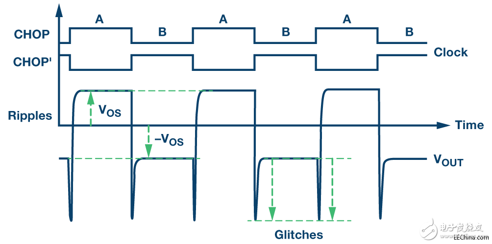
Figure 2. Chopper timing diagram
Switch artifacts in the data sheet
In general, zero-drift amplifiers have large broadband noise and low switching frequencies ranging from a few kilohertz to tens of kilohertz. This limits their use to DC and applications below 100 Hz to keep the switching frequency outside the target signal bandwidth. For applications that require high accuracy and low drift at higher bandwidths, it is important to use a zero-drift amplifier with a high switching frequency. In fact, the switching frequency can sometimes be seen as the quality factor of a zero-drift amplifier. The newer zero-drift amplifiers feature an advanced design architecture designed for smaller switching artifacts at much higher frequencies. For example, in addition to chopping the offset voltage at 4.8 MHz, the high-voltage, dual-channel, zero-drift amplifier ADA4522-2 also features a patented offset and ripple correction loop to minimize switching artifacts. The correction loop operates at 800 kHz and is used to eliminate the offset voltage ±VOS (see Figure 2). Decreasing ±VOS to 1% of its initial value improves 40 dB switching artifacts. This reduces the amount of work required by system designers to achieve system-level accuracy goals.
The easiest way to detect switching artifacts is to look at the amplifier's voltage noise density spectrum. Figure 3 shows the voltage noise density map of the ADA4522-2 folded into the input. Note that Channel B exhibits an increase in the noise spectrum at its 800 kHz switching frequency. As mentioned earlier, this increase in noise spectrum is a side effect of charge injection mismatch. Since the mismatch depends on the device-to-device and channel-to-channel, the magnitude of the noise spikes varies, and not all devices exhibit noise spikes. For example, channel A of the same device does not exhibit any noise spikes at the 800 kHz switching frequency. The switching frequency between devices can vary from 10% to 20%, depending on the frequency of the on-chip clock oscillator.
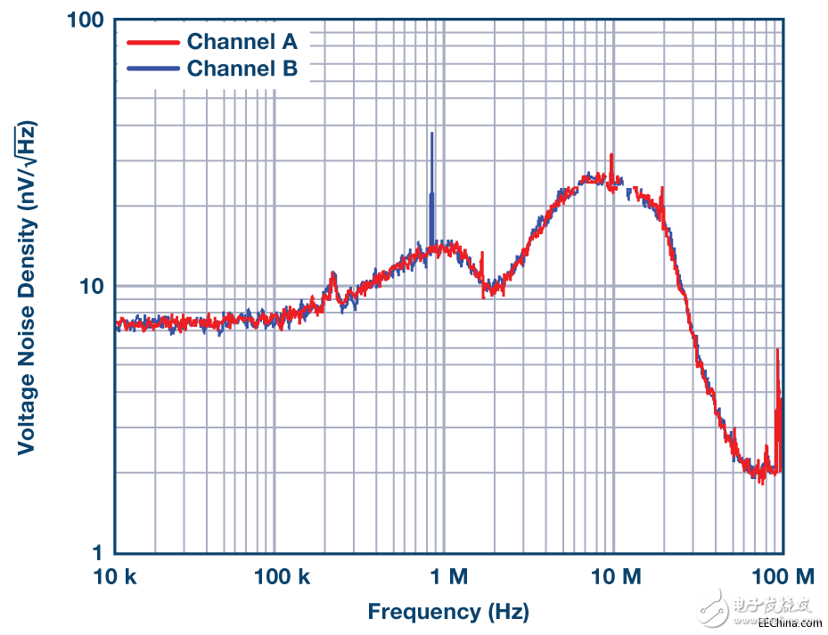
Figure 3. ADA4522-2 voltage noise density
Noise comparison between different zero-drift amplifiers
Figure 4 shows the voltage noise density of three different high-voltage, zero-drift amplifiers folded into the input. Note that all three zero-drift amplifiers tested exhibited some degree of switching artifacts. Some switching artifacts are also repeated at their integer multiples of frequency. These switching artifacts can be very large and can introduce errors into the circuit design. Therefore, it is important to understand their impact on the circuit and then find ways to mitigate the impact. If the amplifier has a closed-loop frequency above the switching frequency, then this increase in noise spectrum is integrated into the entire bandwidth and reflected at the output. Not only that, but the voltage noise that is converted to the input is also amplified by the amplifier noise gain. For example, assuming the amplifier is configured for a gain of 100, the effective noise voltage density that is converted to the output is also increased by a factor of 100.
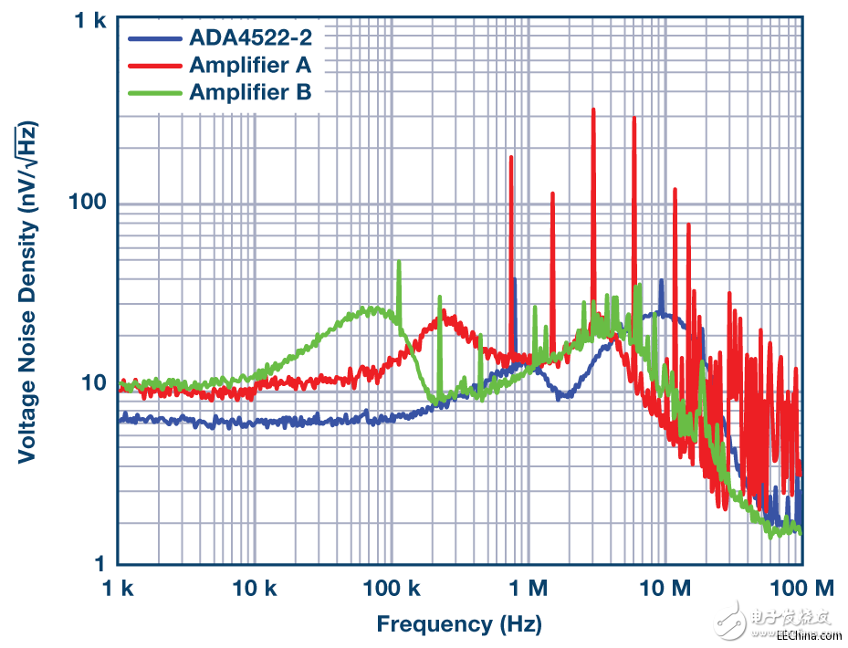
Figure 4. Voltage noise density of different zero-drift amplifiers
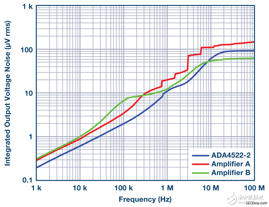
Figure 5. Integrated output voltage noise
The total RMS noise integrated into the amplifier output depends on the amplifier bandwidth. The output voltage noise rolls off with the available bandwidth; therefore, the higher the gain or the wider the bandwidth, the greater the amplitude of the output amplifier noise. Figure 5 shows the integrated output voltage noise versus frequency. This picture is useful for understanding the total integral noise of the relative frequency. For example, if the bandwidth of the amplifier is limited to 100 kHz by filtering, the total output noise due to the inherent voltage noise of the amplifier can be seen from this figure as follows:
Table 1. Output integral noise

Using the general multiplication factor (called the crest factor) to convert the RMS voltage to the peak-to-peak voltage, the peak-to-peak noise predictions are shown in the third column of Table 1. In a 5 V system, the ADA4522-2 provides 18.6 bits of peak-to-peak resolution, while amplifier B provides 16.8 bits of peak-to-peak resolution. A lower total integrated output noise is always necessary because it increases the signal-to-noise ratio and gives the entire system a higher resolution.
Another interesting point to note in Figure 5 is that the integral noise is incremented by a step-like function at the noise spike frequency. Although the noise spike (increased noise energy) is very narrow, it will greatly increase the total output integral noise.
Switching artifacts in the time domain
In many cases, switching artifacts can be clearly seen in the voltage noise density spectrum of the frequency domain. To understand the time-based switching artifacts, you can configure the amplifier as a buffer, ground its non-inverting pins, and observe the output directly through the oscilloscope. Figure 6 shows a typical output of two zero-drift amplifiers. Note that amplifier A exhibits an output voltage spike across multiple amplitudes. The spikes are repeated every 0.66 μs. This matches the noise spike seen at 1.51 MHz in Figure 4. On the other hand, the ADA4522-2 does not exhibit any switching artifacts (blue graphics) in the time domain. In other words, the noise spike is below the noise floor of the measurement system and cannot be measured. This way, designers can use the ADA4522-2 in applications that drive ADCs, and confidently know that noise spikes won't cause any problems.
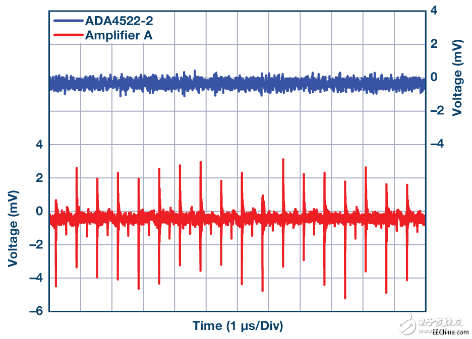
Figure 6. Output voltage noise in the time domain
Filter to reduce switching artifacts
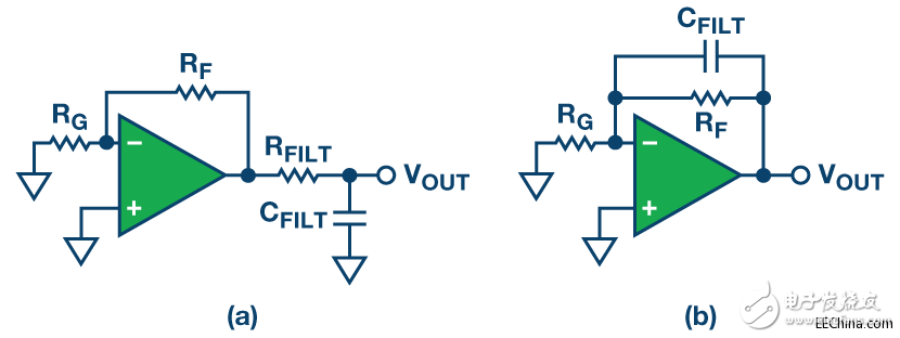
Figure 7. Zero-Drift Amplifier with Filter
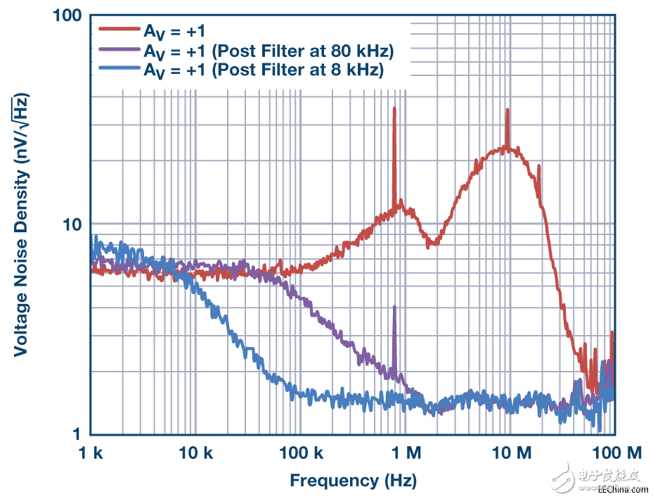
Figure 8. Unity Gain Zero-Drift Amplifier Voltage Noise Density with Post Filter
There are several ways to reduce the effects of switching artifacts. These methods ultimately depend on limiting the amplifier bandwidth to below the switching frequency. Using filters is an effective way to suppress noise spikes. The simplest design is to place a resistor-capacitor network at the output of the amplifier to form a low-pass filter (Figure 7A). Figure 8 shows the voltage noise density of a zero-drift amplifier with a post filter designed to be 10% or 20% below the switching frequency. The noise spike at 800 kHz drops from 36 nV/Hz (without post filter) to 4.1 nV/Hz (post filter is 80 kHz), below the amplifier's low frequency broadband noise level. Since the post filter is located at 20% below the switching frequency (8 kHz for the post filter), the noise spikes are no longer visible, and the ADA4522-2 is identical to any other conventional amplifier.
Some applications may not be able to use an RC network at the amplifier output. The amplifier output current flows through the filter resistor, causing a voltage offset that causes an output error. In this case, you can choose to place a feedback capacitor across the feedback loop to filter the noise spikes (Figure 7(b)). Figure 9 shows the output voltage noise density for an amplifier with a gain of 10, no filtering, and a post filter or feedback filter at 10% below the switching frequency. The post filter configuration is more efficient than a feedback capacitor as a low pass filter.
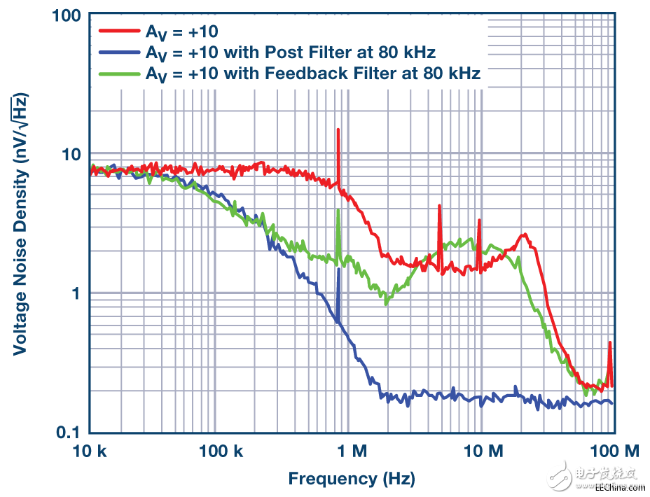
Figure 9. Switching artifacts are reduced with filtering
Using a zero-drift amplifier in a high-gain configuration can help
Many designers use zero-drift amplifiers, but no switching artifacts are observed in the system. Amplifier configuration may be one of the reasons. Zero-drift amplifiers have low drift and offset characteristics and are commonly used to perform signal conditioning on low-amplitude sensor signals in high gain (eg, 100 to 1000 gain) configurations. The effect of using an amplifier in a high gain configuration is the same as placing a low pass filter on the amplifier side. As the gain increases, the bandwidth decreases. Figure 10 shows how a high gain configuration reduces the switching effect. When the closed loop gain is 100, the switching artifacts are barely visible on the noise curve.
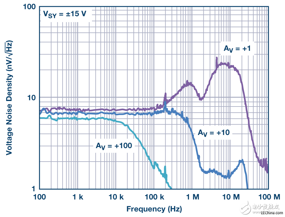
Figure 10. Amplifier Bandwidth Roll-Off with Gain
Advantages of the ADA4522-2 as a Zero-Drift Amplifier
ADI's new zero-drift operational amplifier, the ADA4522-2, features a patented and innovative circuit topology that enables high switching frequencies and minimizes switching artifacts compared to previous products. When the unity gain bandwidth is 3 MHz and the switching frequency is 800 kHz and 4.8 MHz, the gain configuration of 40 is sufficient to filter the switching artifacts without external low-pass filtering. The device features low offset voltage drift (22 nV/°C maximum), low noise (5.8 nV/Hz, gain configuration of 100), low input bias current (150 pA maximum), high common-mode rejection, and power supply rejection Performance is ideal for precision applications such as electronic scales, current sensing, temperature sensor front ends, load cells and bridge sensors, as well as many other drift-critical applications.
in conclusion
Zero-drift amplifiers with extremely low offset voltage and drift are ideal for high-precision amplification applications for low-level signals. Some suggestions for use are provided below.
All zero-drift amplifiers have some degree of switching artifacts that are typically detected in the voltage noise density curve.
The switching artifact amplitudes of different devices are also different.
The maximum difference in switching frequency between devices is up to 20%.
Switching artifacts can be detected in the frequency and time domains. Switching artifacts can cause errors depending on the application.
Zero-drift amplifiers are typically used in high-gain configurations; at this point the bandwidth drops, so switching artifacts in many cases do not cause any problems.
It is important to reduce switching artifacts to reduce the amount of output error. Use a low pass filter (RC post filter or feedback capacitor) to roll down the amplifier bandwidth before the switching frequency to suppress artifacts.
The high switching frequency reduces the filter's requirement for wider, usable, and no artifact bandwidth.
Acknowledgement
Emman Adrados has contributed to the writing of this article and would like to express my heartfelt thanks.
Author
Vicky Wong [vicky.] is an applications engineer at Analog Devices. He joined Analog Devices in 2008 and is responsible for precision amplifiers and voltage reference products. She holds a bachelor's and master's degree in electrical engineering from the University of Illinois at Urbana-Champaign.
Yoshinori Kusuda [yoshinori.] is an IC design engineer in the Linear and Precision Technology group, based in San Jose, California. He is responsible for precision CMOS amplifiers and switched capacitor design. He received his BS and MS degrees in electrical engineering from the Tokyo Institute of Technology in 2002 and 2004, respectively.
Dongguan City Yuanyue Electronics Co.Ltd , https://www.yyeconn.com