Label: FPGA DDS
This article refers to the address: http://
The Arbitrary Waveform Generato (AWG) is a multi-waveform signal generator that not only produces conventional waveforms such as sine waves and exponential waves, but also exhibits a variety of carrier modulations, such as: Frequency modulation, amplitude modulation, phase modulation and pulse modulation. The waveform can be edited by computer software to generate various arbitrary waveforms required by the user. Arbitrary waveform generator implementations include program control outputs, DMA outputs, variable clock counter addressing, and direct digital frequency synthesis (DDS). At present, the development of arbitrary waveform generators is mainly based on DDS technology. Compared with traditional frequency synthesizers, DDS has the advantages of low cost, low power consumption, high resolution and fast switching time. It is widely used in the fields of communication, measurement and electronic instruments. , is a key technology for the full digitalization of equipment.
1 Theoretical analysis of arbitrary waveform generator
1. 1 Introduction to DDS Technology
The concept of DDS (Direct Digital Sy nthesis) was proposed by American scholars J. Tier ncy, CM Rader and B. Gold in 1971. The technology is frequency synthesis from the concept of phase. The main advantages are continuous output phase, large relative bandwidth, high frequency resolution, high programmability, accuracy and stability. DDS technology uses the look-up table method to generate waveforms, and by modifying the data stored in the ROM, arbitrary waveforms can be generated.
1. 2 DDS basic structure
DDS mainly consists of a phase accumulator, a ROM waveform lookup table, and a digital-to-analog converter. The basic block diagram is shown in Figure 1.

Figure 1 DDS block diagram
The linear digital signal is realized step by step by the phase accumulator. The waveform function is stored in the ROM. According to the phase value of the accumulator output as the address, the amplitude quantized value of the waveform function stored in the ROM is searched, and the phase to amplitude conversion is completed. Corresponding sequence.
2 hardware circuit design
2. 1 design plan
The DDS function is implemented based on the FPGA, and the control is realized by the single chip microcomputer. The core of this solution lies in the design and implementation logic function of the FPGA. After the table is looked up by the memory, the output signal is converted into the required waveform by the connected digital-to-analog converter. The microcontroller is a controller that is easy to control and debug. The system block diagram is shown in Figure 2.

Figure 2 system block diagram
2. 2 use of D / A converter
This case uses Texas Instruments' TLC7528. It is a two-way, 8-bit D/A converter. The design of this case is as follows: The digital control of channel A controls the voltage output of channel B, and the channel of channel B controls the amplitude of the output. The circuit diagram shows that the A(B) voltage input at VA1 (VOB1) is -5~0 V, and the voltage at A(B) is VA2 (VOB2) is -5~5 V. The DA circuit connection diagram is shown in Figure 3.
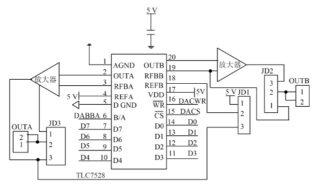
Figure 3 TLC7528 circuit connection diagram
Because of the problem of the conversion method, the generated zero error can be calibrated by adjusting the zero point of the amplifier; and the temperature drift error due to the temperature change is technically difficult to eliminate. The gain error for a unipolar DAC can be eliminated by adjusting the closed-loop gain of the amplifier.
2. 3 filter design
In general, the elliptic filter has the highest sensitivity. When using the same order, the elliptical filter can get the best rectangular coefficient. The 7th-order elliptic filter can get 40 dB out of band at the frequency near the passband. Suppression, very suitable for filtering spurious signals. Another type of waveform output by DDS is an arbitrary waveform with complex spectrum, low frequency, rich spectral structure, high harmonic content, and equal ripple error linear phase filter for filtering. It has a fixed range in a wide range. Delay, at a distance away from the cutoff frequency, its amplitude response is also better.
2. 4 design of single chip microcomputer
The single-chip microcomputer adopts the traditional 8051 single-chip microcomputer, the crystal oscillator is 12 MHz, and the internal oscillation mode is adopted; the reset input pin is active high, and the high level of 2 or more machine cycles can be used to reset the single-chip microcomputer; the MAX232 chip is used as the serial port. The chip and the single chip communicate with other computers or peripheral devices through the asynchronous communication serial interface.
3 FPGA-based DDS implementation
The FPGA chip uses ALT ERA's CYCLON E series EP1C3T 144C8. The design uses Altera's Quar tus, using AS mode and JTAG configuration.
3. 1 fixed waveform output
This case uses several 8 b ROMs with a memory depth of 1,024 points for storing waveform data such as sine waves. Each waveform data is stored in a fixed ROM, such as Sine_ROM, Square_ROM, etc., corresponding to sine, square wave and other storage modules. The waveform of any module is selectively read by an enable module control in an active-low mode. When the waveform is output, only a single ROM is operating, and the other modules are high, ensuring that the desired fixed waveform is output. The input of the enable module is a determinant keyboard, which is set to: One button controls a certain waveform output.
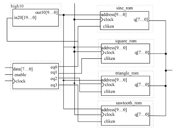
Figure 4 waveform ROM and enable control design circuit diagram
3. 2 arbitrary waveform output
The arbitrary waveform is the waveform data transmitted by the host computer. It is controlled by the single-chip microcomputer. It is necessary to design a RAM that can receive data updates at any time. As shown in Figure 5.
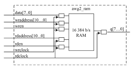
Figure 5 Arbitrary waveform module design circuit diagram
The selected D/A converter is 8 bits, so the word length of the RAM is also 8 bits, so the number of bits of the address line of the waveform RAM is 10 bits. In order to update the arbitrary waveform data, the waveform RAM is designed as a dual port RAM.
4 performance and error analysis
4. 1 test results
The output waveform is shown in Figure 6. The instruments used in this system test are:
Oscilloscope T ekt ronix Company Model: T DS1012
Counter Chuangrui Technology Co., Ltd. Model: SPF40
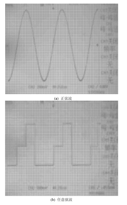
Figure 6 output waveform
4. 2 Frequency measurement
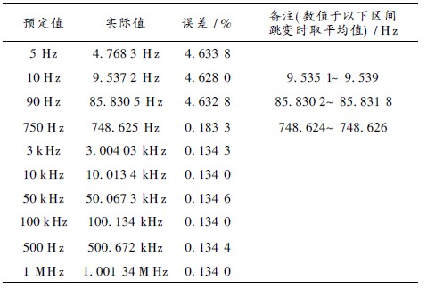
By setting a predetermined value, the actual value is measured by a counter, and the error is calculated based on this data as shown in the following table (only 10 sets of data are selected).
It can be seen from Table 1 that the 1 ~ 100 Hz interval error is more obvious, and the output frequency is stable from 1 kHz to 1 MHz (this table is for testing sine wave data).
Table 1 Frequency data table
4. 3 Error and spurious analysis
In addition to factors such as the working environment and power supply noise, which are factors affecting the purity of the spectrum, there are the following main reasons:
(1) Phase truncation produces spurious signals. The hardware cannot meet the 20-bit data storage. The design uses the high-bit truncation method. Only the upper bits of the accumulator output are used for table lookup, and the low bit is discarded. It will inevitably cause errors and affect the final output signal spectrum. The cosine component is introduced on the sinusoidal signal, causing the superposition in the time domain to appear as a spur in the frequency domain.
(2) Spurious components caused by nonlinearity of the D/A converter. The effect of an ideal DAC on DDS is only manifested by changes in the amplitude and phase of the signal spectrum. The output exhibits roll-off characteristics and does not introduce other frequency components, rather than the ideal DAC nonlinearity, instantaneous glitch, etc. The conversion characteristics create spurs in the output spectrum.
(3) The spurs generated by the quantization of the amplitude. The waveform code stored in the sine lookup table is a value obtained by uniformly divising an analog signal. The capacity of the memory is limited, and it is impossible to record the sine value with an infinite binary number, so amplitude quantization error occurs.
The method of reducing the spurs and noise in the DDS output voltage, in addition to selecting a D/A converter with excellent performance and exquisite workmanship, to improve the digit length and amplitude quantization word length, can also be designed through a well-designed low-pass filter. Filter out various spurious and out-of-band noise, DDS+ PLL frequency synthesis technology, and data compression method with a maximum compression ratio of 128 1 . In addition, high-frequency jitter (Dither) can be added to the generated phase word sequence, because the phase-intercept error is periodically distributed, which will result in large glitch at certain frequencies, making the spectrum generated by DDS free of clutter dynamic range. Reduced. By adding jitter to the phase, the more pronounced periodic distribution in the phase error can be destroyed, so that the amplitude of the glitch is reduced, and the clutter-free dynamic range of the output sine cosine wave is increased.
A phase error feedback structure can also be used to add a second-order FIR filter ( Finite Impulse Response) to the SCMF (phase accumulator and sine and cosine function generator) to filter out the phase error near the output frequency.
5 Conclusion
The design of the arbitrary waveform generator is one of the classic topics in the national electronic design competition. The design of the arbitrary waveform generator not only has a wide range of practical application space, but also has the improvement of the student's hands-on ability and the integration of subject knowledge in the electronics department. Great guiding value. This paper seeks the design effect of powerful function, convenient operation and stable output parameters, and mainly focuses on the basics, making it more in line with the typical teaching conditions of textbooks, and measuring the relevant parameters to analyze the reasons. Regarding the design of the waveform generator, there are still many functions that can be designed and extended, and there are still many methods worth exploring in the weakening of the spurs.
Network Cable
Wisesir network cable include many types of cable,such as Usb Printer Cable,Patch Cord,audio and Video Cable,ethernet cable,rj45 cable,etc..

Waireless Power Bank,Usb Printer Cable,Mtp Fiber Optic Patch Cord,Video Cable Vga Cable
Pogo Technology International Ltd , https://www.pogomedical.com