The Cd4093 consists of four 2-input Schmitt trigger circuits. Each circuit is a 2-input NAND gate with Schmitt trigger function on both inputs. Each gate opens and closes at a different point on the rising and falling edges of the signal. The difference between the rising voltage (V P )T and the falling voltage (V N ) is defined as the hysteresis voltage
(â–³V T ).

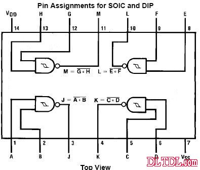
CD4093 pin diagram
CD4093 pin function:
A data input terminal E data input terminal J data output terminal B data input terminal F data input terminal K data output terminal C data input terminal G data input terminal L data output terminal D data input terminal H data input terminal M data output terminal VDD positive Power VSS ground --
Absolute Maximum Ratings Absolute Maximum Ratings:
DC Supply Voltage DC Supply Voltage (VDD) -0.5 to +18 VDC Input Voltage Input Voltage (VIN) -0.5 to VDD +0.5 VDC Storage Temperature Range Storage Temperature Range (TS) -65°C to +150°C Power Dissipation Power Consumption ( PD) Dual-In-Line Normal Double Row Package 700 mW Small Outline Small Outline Package 500 mW Lead Temperature Soldering Temperature (TL) Soldering, 10 seconds) (welding 10 seconds) 260°C
Recommended Operating Conditions Recommended Operating Conditions:
DC Supply Voltage DC Supply Voltage (VDD) 3 to 15 VDC Input Voltage Input Voltage (VIN) 0 to VDD VDC Operating Temperature Range Operating Temperature Range (TA) -40°C to +85°C
DC Electrical Characteristics DC Electrical Characteristics:
Symbol symbol
Parameter parameter
Conditions Conditions -40°C +25°C +85°C
Units unit
Typically Min Max Min Max Min Max quiescent current IDD Quiescent Device Current VDD = 5V 1.0 1.0 7.5 μA VDD = 10V 2.0 2.0 15.0 VDD = 15V 4.0 4.0 30.0 VOL LOW Level Output Voltage Output Low Voltage VIN = VDD, | IO | < 1μA VDD = 5V 0.05 0 0.05 0.05 V VDD = 10V 0.05 0 0.05 0.05 VDD = 15V 0.05 0 0.05 0.05 VOH HIGH Level Output Voltage Output high level voltage VIN = VSS, |IO| < 1μA VDD = 5V 4.95 4.95 5 4.95 V VDD = 10V 9.95 9.95 10 9.95 VDD = 15V 14.95 14.95 15 14.95 VT- Negative-Going Threshold Voltage (Any Input) Negative threshold voltage (any input) |IO| < 1μA VDD=5V, VO =4.5V 1.3 2.25 1.5 1.8 2.25 1.5 2.3 V VDD=10V, VO = 9V 2.85 4.5 3.0 4.1 4.5 3.0 4.65 VDD=15V, VO=13.5V 4.35 6.75 4.5 6.3 6.75 4.5 6.9 VT+ Positive-Going Threshold Voltage (Any Input) Forward threshold voltage (any input ) | IO| < 1μA VDD = 5V, VO = 0.5V 2.75 3.6 2.75 3.3 3.5 2.65 3.5 VVDD = 10V, VO = 1V 5.5 7.15 5.5 6.2 7.0 5.35 7.0 VDD = 15V, VO = 1.5V 8.25 10.65 8.25 9.0 10.5 8.1 10.5 VH Hysteresis (VT+ - VT-) (Any Input) Hysteresis (VT+ - VT-) (any input) VDD = 5V 0.5 2.35 0.5 1.5 2.0 0.35 2.0 V VDD = 10V 1.0 4.3 1.0 2.2 4.0 0.70 4.0 VDD = 15V 1.5 6.3 1.5 2.7 6.0 1.20 6.0 IOL LOW Level Output Current Output Low Current (Note 3) VIN = VDD VDD=5V, VO =0.4V 0.52 0.44 0.88 0.36 mA VDD=10V, VO=0.5V 1.3 1.1 2.25 0.9 VDD=15V, VO =1.5V 3.6 3.0 8.8 2.4 IOH HIGH Level Output Current Output high level current (Note 3) VIN = VSS VDD=5V, VO =4.6V -0.52 0.44 -0.88 -0.36 mA VDD =10V, VO=9.5V -1.3 -1.1 -2.25 -0.9 VDD=15V, VO=13.5V -3.6 -3.0 -8.8 -2.4 IIN Input Current Input current VDD=15V, VIN = 0V -0.3 -10 -5 -0.3 -1.0 μA VDD=15V, VIN =15V 0.3 10 -5 0.3 1.0
AC Electrical Characteristics AC Electrical Characteristics:
Symbol symbol
Parameter parameter
Conditions
Minimum Typical Maximum
Units unit
tPHL, tPLH Propagation Delay Time Transfer delay time VDD = 5V 300 450 ns VDD = 10V 120 210 VDD = 15V 80 160 tTHL, tTLH Transition Time transition time VDD = 5V 90 145 nsVDD = 10V 50 75 VDD = 15V 40 60 CIN Input Capacitance Input Input (Any Input) 5.0 7.5 pF CPD Power Dissipation Power Capacitance (Per Gate) 24 pF Typical Application Circuit:

Negative edge trigger

Positive edge trigger

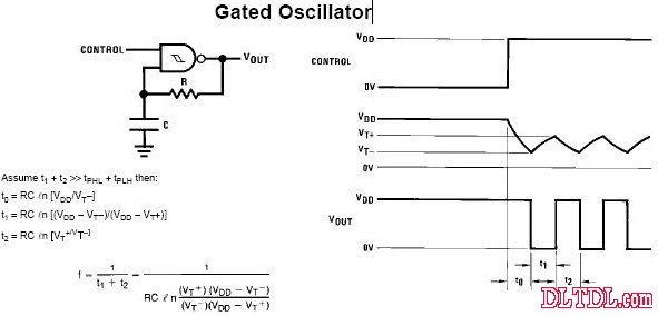
Controlled oscillator
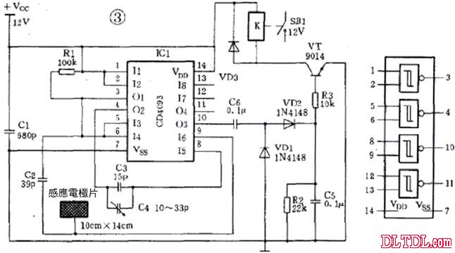
Application circuit: touch switch

The circuit is mainly composed of a four-two input NAND gate integrated circuit CD4093. A NAND gate (1, 2, 3, IC1) of R1, C1 and CD4093 constitutes a 400Hz square wave oscillator, and the square wave of the oscillator output is divided into two paths: one way is directly sent to a NAND circuit (4, 5) , 6 feet, IC2); the other way is sent to a NAND gate (8, 9, 10, IC3) via a capacitor C2. Since IC2 is connected in the form of a NOT gate, its input and output potentials are 180° out of phase, and the signal output from IC2 is coupled to the other input of IC3 via C3 and C4.
Since the levels of the two inputs of IC3 are the same. The phase is opposite, so as long as IC1 oscillates normally, at least one of the two inputs of IC3 is at a low level, so the output of IC3 is a stable high level. Due to the action of C6, VT1 is turned off. However, if the input signal of any input of IC3 is canceled or the amplitude of the signal is lowered below the input start level of the gate, IC3 outputs a square wave signal.
When a conductor approaches the sensing electrode, part of the signal coupled by C2 to the input pin 9 of IC3 is shunted to ground. If the amplitude of the signal after shunting is lower than the threshold level of the NAND gate, IC3 The square wave signal is output. After the signal is rectified by VD1 and VD2, the switching tube VT1 is turned on, and the power of the relay is turned on to make it close.
Capacitor C4 is the sensitivity adjustment capacitor. If the circuit needs to work with maximum sensitivity, you can adjust C4 to make the relay just pick up, then adjust C4 to make the relay just disconnect, then seal C4 with high frequency wax or insulating paint. .
The texture of Regular Back Sticker attracts you in a unique and innovative way. The ultra-thin and breathable material does not affect the heat dissipation function of the device at all. The smooth feel and personalized patterns not only protect the phone from scratches, dust, impacts and fingerprints. Bring you a different experience.
The Back Film protects the back cover of the phone from unnecessary scratches and repels dust, while reducing the signs of daily wear and tear.
It has oleophobic and waterproof effects, which can prevent the adhesion of oil stains and fingerprints. Provide comprehensive protection and maintain a new state.
Using the Protective Film Cutting Machine, you can install the Back Film on different types of mobile phone back shells, including mobile phones, tablets and other electronic products. With just one click, the customization can be completed in 30 seconds.
If you want to know more about Regular Back Sticker products, please click the product details to view the parameters, models, pictures, prices and other information about Regular Back Sticker products.
Whether you are a group or an individual, we will try our best to provide you with accurate and comprehensive information about Regular Back Sticke!
Leather Back Sticker, Aurora Back Sticker, Back Skin Sticker, Brushed Metal Back Sticker, Mobile Phone Sticker, Back Sticker,Mobile Skin Sticker
Shenzhen Jianjiantong Technology Co., Ltd. , https://www.jjtbackskin.com