Digital Signal Processing (DSP) is an emerging discipline that involves many disciplines and is widely used in many fields. Since the 1960s, with the rapid development of computer and information technology, digital signal processing technology came into being and has developed rapidly. In the past two decades, digital signal processing has been widely used in the field of communications and other DSP technology illustrations. Digital signal processing is to use a computer or special processing equipment to collect, transform, filter, estimate, enhance, compress, and identify signals in digital form to obtain a signal form that meets people's needs.
This article brings you the design scheme sharing of audio signal filtering system based on DSP chip.
Hardware designThis system uses the DSP chip TMS320C5416 and TLV320AIC23 audio codec chip to realize the system's hardware and software design, and on this basis, complete the voice signal collection, playback, storage, analysis functions. The article includes 3 parts: audio signal acquisition, DSP chip processing signal, Flash memory. The overall design structure of the system is shown in Figure 1.
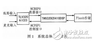
TMS320C5416 is the main chip used in the article. It is a low-power, high-performance DSP chip. Its main functions include collecting voice signals, storage, and communication between control modules. The audio signals are collected and compressed and stored in Flash memory. Does AIC23's high-performance stereo signal input support MIC and LINE? IN two ways, configurable register selection, and programmable gain adjustment. It internally integrates analog-to-digital and digital-to-analog conversion components, adopts advanced sampling technology, and the sampling range is between 8K and 96K.
This design's slave chip TLV320AIC23 audio codec chip is a stereo audio Codec chip, which is mainly responsible for A / D conversion, sampling encoding and filtering of voice signals. The chip is an ideal audio analog device and is widely used; three DSP chips There are two buffered serial ports MCBSP0 and MCBSP1 responsible for controlling the audio chip AIC23. Among them, the MCBSP0 serial port is an SPI interface to realize the transmission and reception of voice data. The MCBSP1 serial port is an I2S interface. The task is to write control words; the Flash storage module can quickly access the erasable Write, memory that will not lose data even if the power is off, and the cost is low, the reliability is high, the stability is strong, the capacity is several GB, the appearance is small and other characteristics, read and store operations as the carrier.
System hardware circuit designThe DSP chip TMS320C5416 used in this system, the highest frequency can reach 160MIPS, the system has good real-time performance; the audio codec chip TLV320AIC23 has a sampling accuracy of 16 to 32 bits. The combination of the above two chips is an ideal design for solving mobile audio recording and playback systems and collecting voice on site. The three MCBSPs of TMS320C5416 can easily realize the control and communication between AIC23. AIC23 is a programmable chip, which contains 11 16-bit registers. The MODE pin selects the SPI or I2C working mode of the control interface. MODE = 0 adopts I2C mode; MODE = 1 represents SPI mode.
AIC23 independent control port receives the command word of the controller, and an independent data interface exchanges DSP voice data. It is 12M external crystal oscillator that provides working clock for DSP. In this system, MCBSP0 of C5416DSP is connected to the control interface of AIC23, and MCBS P1 is connected to the data interface of AIC23. The interface block diagram of TMS320C5416DSP connected to TLV320AIC23 is shown in Figure 2.

This design uses TMS320C5416 chip, its internal 128K * 16 RAM, can effectively improve the system integration and overall performance. In addition, it has 3 multi-channel buffered serial ports, providing 128 channels. The characteristics of the C5416 chip are: operating frequency up to 160 MIPS; 64K of data storage space and 64K of I / O space that can be accessed.
The pins connected by TMS320C5416 and TLV320AIC23 are as follows: BCLKX0 / 1: transmission clock signal, which is the serial shift clock signal of the multi-channel buffered serial interface transmitter. When reset, it defaults to input. When OFF is low level, BCLKX enters high configuration; when TMS320C5416 is connected to FLASH device, the DSP chip collects 32-bit voice data each time, and then writes to the Flash device from the left channel to the right channel for storage.
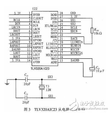
TLV320AIC23 voice acquisition and playback interface circuit moduleThe AIC23 chip integrates the ADC and DAC, compatible with the input / output voltage of the C5416, and its digital interface is seamlessly connected to the MCBSP port of the DSP. AIC23 adopts advanced Sigma-delta oversampling technology to transfer most of the noise to the resistance state. The sampling frequency range is 8K to 96K and provides 4 kinds of 16 bit, 20 bit, 24 bit and 32 bit sampling data. The output of ADC and DAC The signal-to-noise ratio reaches 90 dB and 100 dB, respectively.
The pin diagram of TLV320AIC23 and TMS320C5416 connection is as follows. BCLK: I2S digital audio interface clock signal, serial data transmission clock, when the main mode is AIC23, ACLK23 generates BCLK and transmits it to the DSP, the frequency at this time is only 1/4 of the main clock, when in the slave mode, DSP generates BCLK; DIN: I2S format input to D / A converter; DOUT, stereo ADC generation, I2S format A / D converter serial data output: LRCIN / LRCOUT: I2SD / A and A / D converter word clock signal , In master mode, AIC23 generates this signal and sends it to DSP. In slave mode, it is generated by DSP; SCLK: serial clock input of control port; SDIN: serial data input of control port, control protocol, transmission configuration data; / CS: In SPI mode, it is the data latch control terminal, in I2C mode, as the last bit of the peripheral 7-bit address; XTI / MCLK: external clock input. In this paper, AIC23 is provided with an external crystal to provide a working clock, and the TLV320AIC23 slave circuit module circuit is shown in Figure 3.
The voice data storage module in this paper uses 32M * 8-bit Flash storage space, which can meet the capacity of the memory chip and the speed of reading the voice signal. The flash memory stores the recording and playback system data. Flash is composed of a group of 1KB blocks that can be erased independently. Erasing a block will reset all the blocks to 1. The base address of each block of the flash memory is fixed. Flash memory is at the starting position in the memory, generally starting from 0. Figure 4 below is the circuit diagram of the Flash memory module.
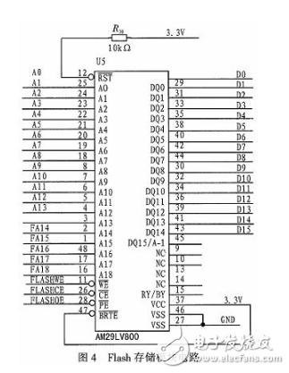
Flash memory is a kind of non-volatile memory, and its storage characteristics are equivalent to hard disks, so it becomes a storage medium for portable digital devices. At the same time, Flash memory uses a serial structure, and the reading and writing unit is in units of pages and blocks. The capacity can be large and the cost is low. , And can ensure the accuracy of data reading and writing. The I / O port of the flash memory has 8 bits, and the method of data transmission is to transmit the command word in turn. The 32-bit voice data collected by the DSP is divided into 4 times through the external bus and written into the flash memory from the left to the right channel.
Power interface moduleThe power supply structure of TMS320C5416DSP adopts dual power supply device chip, core power supply CVDD and I / O power supply DVDD, relative voltage and power-on sequence need to be considered. The two power supply control strategies are different: DVDD is powered by a single 3.3 V power supply, and CVDD is only loaded with 1.6 V. To reduce power supply, we want to reduce the power consumption of the chip. Dual power supply mode can eliminate the delay between power supplies. In an ideal state, I / O power and core power should be powered on at the same time, but in reality it is not easy to do so. If you can't power up at the same time, you need to configure the operating mode according to the pin level. The core must give priority to I / O power supply, requiring one voltage to be lower than the operating voltage, and the other voltage supply time cannot exceed the requirement. During the power-on process, it is necessary to ensure that the I / O buffer receives the correct core output and to prevent the system bus conflict. The power-up sequence mainly depends on the internal electrostatic protection circuit as shown in Figure 5.
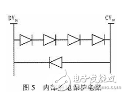
It can be seen from the figure that DVDD is required to not exceed CVDD 2 V, so 4 diodes are used for buck, and the core power supply cannot exceed the I / O power supply voltage of 0.5 V, so only one diode is used, otherwise the chip will be easily damaged.
System software design moduleThe software environment of this voice recording and playback system is a DSP integrated development environment IDE that provides mature core functions and convenient graphical visualization tools, making the design faster. CCS2.0 provides a graphical interface, with editing tools and project management tools, providing software development, program debugging and simulation environment, integrating assembler, compiler, library building tools, etc. CCS integrated code debugging tool has various debugging functions, and supports assembly and C / C ++ language. The program software of this system is written in C language. It is not only easy to debug, but also can improve the execution efficiency of the software, and can perform instruction level simulation and real-time data analysis on the DSP. It also has rich library functions.
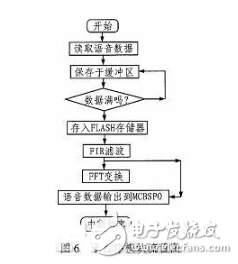
The software part of the system mainly collects and stores the signals collected from the field line input and microphone voice into the Flash memory, broadcasts the signals after filtering, and transforms the signals into the frequency domain, that is, FFT discrete Fourier fast transform.
Voice analysis submoduleThe voice signal input at the scene is sent to the stereo audio codec AIC23. The AIC23 controls the on-chip registers, converts the signal A / D, processes the digital signal with a digital computer, then filters it with a digital filter, and sends it to the flash memory for temporary storage. The digital filter is a discrete-time system. Process of the program voice module: first initialize the system, including setting the clock generator, AIC23 initialization, multi-channel buffering, working variable initialization, etc.
Voice analysis program module processing process: TLN320AIC23 is initialized, the voice recording data is read and stored in the data buffer, and the FIR digital filter is called to filter, the effect is outstanding, then the digital voice signal is temporarily stored in the flash memory, and finally sent out by the headset, while performing FFT Discrete fast transform algorithm. Voice data is output to MCBSP. The flow chart of voice analysis subroutine module is shown in Figure 6.
The finite length of the window function is used to realize the windowed linear phase FIR digital filter, which can meet the common problems of transfer sequence or impulse response.
b = fir1 (n, Wn, 'ftype');
b = fr1 (n, Wn, 'ftype', 'window');
n is the order of the filter, Wn is the cut-off frequency, ftype determines the filter type, high-pass filter when high, and band-stop filter when stop. window adopts the window function type, which is a design method that makes the infinite-length non-causal sequence into a finite-length impulse response sequence through truncation and weighting. An n-point Hamming window function. Write matlab program, generate FIR coefficient and store it in FH [n], and display the result in the display area after the program runs.
FFT is an efficient method to quickly calculate DFT, which can significantly reduce the amount of calculation and greatly improve the speed of DFT calculation. Most DSP chips can complete multiply-accumulate operations within a single instruction cycle. The FFT algorithm uses the characteristics of DFT coefficients to combine operations to convert long sequences into short sequence DFT to reduce the amount of calculation. The realization process of FFT algorithm:
1) Decompose the N-point time-domain signal into N time-domain signals, make up the signal at a single point, and calculate the frequency spectrum.
2) The bit reversal of the input data is to arrange the input sequence into the reverse order of the bit sequence. Bit code inversion can improve program execution speed and storage efficiency.
3) Implement N-point complex FFT, perform three loop sets to calculate FFT transform, and perform butterfly operation at the innermost layer. The first, second, third to log2N stages are all butterfly operations. The number of sequence points N = 2m, N is an integer power FFT algorithm of 2.
4) Estimated power
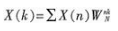
X (k) is generally divided into an imaginary part and a real part, and the data transformed by the FFT algorithm is used to calculate the square sum.
Control register programmingThis article's TLV320AIC23 uses serial transmission of data. The first half of the data control needs to store the register address, and the second half saves the value to be written in the register. Two 8 bits are used to process serially transmitted control data. Combined with the actual situation, this article uses assembly language for the I2C writing module.
DSP sends the configuration command to AIC23 through the I2C bus to complete the initial configuration, and then AIC23 starts to work. The initialization of AIC23 is recorded in an array, and the commands are sent through the serial port and sent in a cyclic manner. The timing diagram of AIC23 data writing is shown in Figure 7.
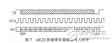
As shown in the figure B [15 ~ 9] is the address of the record control register, B [8 ~ 0] is the value to be written is saved in the register.
Dongguan Tuojun Electronic Technology Co., Ltd , https://www.fibercablessupplier.com