The frequency response of the flyback converter operating in voltage mode control (VM) and driving in continuous conduction mode (CCM) is a secondary command system. If most of the analysis predicts that the quality factor of the transfer function is only affected by various losses (ohmic path, magnetic loss, recovery-time related loss, etc.), the damping effect caused by the leakage inductance is very small. However, the transient simulation predicts that the output damping will oscillate as the leakage inductance increases. Since the formulas in the existing literature do not reflect this effect, it is necessary to adopt a new model, which will be described in this paper.
Flyback Converter in CCM
An ideal CCM flyback converter transmits power over two duty cycles:
1) On-time ton, during which the primary-side power switch SW is closed and energy is concentrated on the primary inductance Lp of the transformer.
2) During the off time toff, the switch is open and energy is transferred through the diode D to the secondary side. However, when examining the prototype waveform, more cases than the basic interpretation description can be distinguished. Figure 1 shows a typical converter using a transformer affected by leakage inductance, lleak. When the power switch is turned off, an input voltage is applied to the primary inductance Lp of the transformer, and the ohmic loss of the switch is negligible. Looking closely at this schematic, this is not an exact Vin, because Lp and lleak separate a portion of the voltage. Therefore, the voltage of Lp at this time is
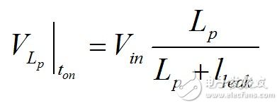
(1)

Figure 1: Flyback converter operating state display When the power switch is turned on, energy is stored on the primary side, and then the energy is cycled on the secondary side
During ton and taking into account the coupling point, the secondary diode is blocked. Since Lp and lleak are connected in series, the current ip(t) in these components increases, and the slope is
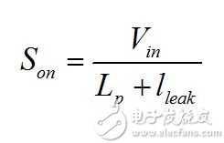
(2) When the controller indicates that the switch is on, we jump to Figure (b). At this point the induced current finds a path in the capacitance of the drain node. The parasitic parameters consist of the MOSFET's own non-linear capacitors Crss and C oss at the drain terminals, plus the various capacitances of the clamp diodes, the transformer winding-to-winding capacitance, and the output diode capacitance reflected to the primary. All these elements are collectively referred to as ground reference capacitors, defined as Clump. When the current flows through Clump, the drain-source voltage increases rapidly. Due to the nonlinear capacitance of the MOSFET, the slope is not constant. But we can say that the slope of this voltage is approximately
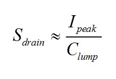
(3) where Ipeak is the current value when the switch is open. The drain voltage increases until the Lp voltage reverses. At this point, as in Figure 1c, the secondary diode is biased but no current is flowing at the secondary. When both Lp and lleak are energized, current is drawn to the lumped capacitance that is continuously charged. Since it is in series, the currents of Lp and lleak are equal, and the net current flowing through the secondary diode is zero. D starts to conduct the drain voltage
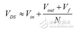
(4) The output voltage is now flyback to Lp - hence the flyback converter - and produces a downward slope
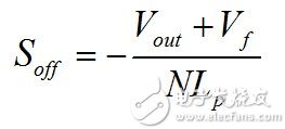
(5) The drain node continues to increase until the input voltage plus clamp level Vclp is reached. The clamp diode is turned on at this time, as shown in Figure 2a. When the drain node voltage stays at Vin + Vclp, the leakage current no longer flows through Clump but only Vclp. The charge of the lumped capacitor absorbs the leakage inductance energy, and the circulating current in Vclp is now slightly less than the initial peak primary current.
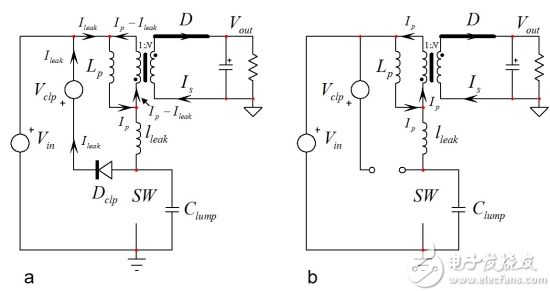
Figure 2: When the lumped capacitor is charged to Vin + Vclp, the clamp diode turns on.
When the switch is opened with a peak current I p1 , the total energy stored in the circuit is
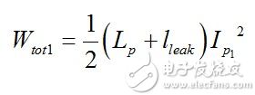
(6) When the clamp diode starts to conduct, the energy stored in the lumped capacitance is
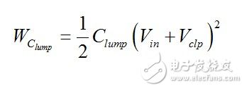
(7) At this point, the energy stored in the circuit now includes lumped capacitance:

(8) where I p2 is the circulating current after charging the lumped capacitors. The number of energies in equation (6) does not change, except that part of it has been passed to Clump. thus,

(9) Refresh

(10) Solve I p2 from this expression

(11) Assume the following values

Then the current drawn from (11) is about 976 mA or 2.4% less than the initial 1 A peak current when the switch is turned on. Please note that Clump is a highly non-linear item, especially the low voltage point when the switch is turned on. If (11) is an approximate theoretical formula, the bench test verifies that the current circulating in the clamp network is lower when the diode Dclp starts to conduct. Increasing the capacitance at the drain with an additional 100-pF capacitor (1 kV for off-line applications) will further reduce the current. This extra capacitance facilitates the residual current device (RCD) clamping temperature and reduces turn-off losses by buffering the drain voltage. By reducing the node's dV/dt, EMI will also improve. However, adding this capacitor may limit the high linear conduction loss budget if the switching frequency is high. Must consider for compromise.
At this point, the leakage inductance voltage is fixed (ignoring the ripple): the lower terminal is held at Vin + Vclp (ignoring clamp diode drop), and the upper terminal is Vin + (Vout + Vf)/N. The voltage applied to the leakage inductance is therefore Vclp-(Vout+Vf)/N. The reset time of the leakage inductance starts here. The current defined by (11) falls, the slope
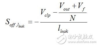
(12) When the leakage inductance is reset, the secondary-side diode current id (t) is generated with the slope defined by (12), but this time is positive and increases by the turns ratio. When the leakage inductance is completely depleted, the output diode current peaks (Figure 2b). The secondary current now decreases with the slope defined by equation (5). This falling slope continues until the switch opens again. This is the off time description toff. However, the output diode current cannot immediately return to zero. The reason is that it takes time to stimulate the leakage inductance: its current must jump to the primary inductor and still couple to the secondary side. This is the time for the switch current to increase from 0 to the valley current Iv. When ISW ​​= Iv, all primary currents now flow through the power switch and the secondary diodes are blocked. Two important points can be inferred from this information:
1. When the switch is open, the secondary diode remains on for a period of time t1. This is the time when the leakage current increases from 0 to the valley current Iv. Since the output diode is always on for a short period of time, Lp demagnetizes: the leakage inductance lengthens the conduction time of the secondary diode. Although the switch is off, the primary inductor slope does not change until the leakage inductor current reaches the valley current and the overall flow to the ground: the duty cycle D decreases by d1.
2. When the switch SW is turned on, the net current of the secondary diode is 0, and all the primary currents are shunted by the leakage inductance Clump. When the leakage inductance resets, the secondary current rises and peaks at the completion of the reset: the leakage inductance delays the time t2 of the secondary current generation and affects its peak value. The energy stored in the leakage inductance plus the extra energy of the primary inductance is consumed in the clamping network.
The close-up of this event is shown in Figure 3. As you can see, the leakage inductance is significantly delayed and prevents the secondary current from peaking immediately. Also, this peak current is not Ipeak/N, but as shown in [1]
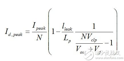
(13)
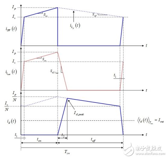
Figure 3: When the leakage inductance is depleted, the secondary-side current peaks.
Update Dc transfer function
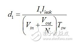
Now that we have a better understanding of the conversion process, let us calculate the small time events t1 and t2 that have been described. T1 is the time required to drive the leakage inductance from 0 to the valley current Iv. When SW turns off, the voltage applied to the leakage inductance is the reflected output voltage (the diode D is still on) and the input voltage Vin. The secondary diode forward voltage drop, Vf, is ignored, so the time t1 is defined as:
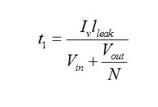
(14) If we normalize to the switching cycle, we get the duty cycle d1
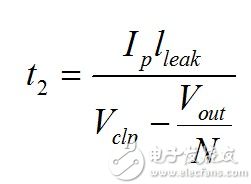
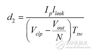
(15) The leakage inductance reset time t2 is determined in a similar manner. When the switch is turned on (ignoring the charging time of the lumped capacitor), the voltage applied to the leakage inductance is the clamped level anti-reflection voltage since D starts to conduct. So we have
(16) Once normalized to the switching period, we find that the duty cycle d2 is
(17) A good tool to determine the output voltage of the converter is the inductor charge balance method, which states that the average voltage of the inductor L at steady state is zero:
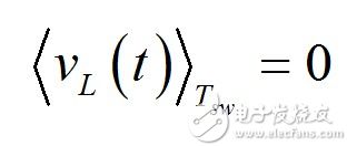
(18) The primary inductor voltage is shown in Figure 4. To comply with (18), we can write the following equation

(19) Solve Vout in the above expression and rearrange it to

(20) Simplified to
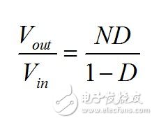
(21) Leakage inductance is 0 at this time.
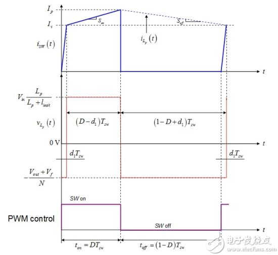
Figure 4: The average voltage of the primary inductor at steady state is 0.
The observation we are interested in is the effective on-time – during which the primary inductor slope is positive – it is actually a reduction in DTsw. The effective duty cycle further decreases as the leakage inductance increases. The voltage applied to the primary inductor is also not Vin, but smaller, as in equation (1).
Simple cycle-by-cycle model
To test our calculations and waveforms, we have collected a simple flyback converter operating at a 40% duty cycle, providing slightly more than 60 W of power. The electrical diagram is shown in Figure 5. The leakage inductance has been set to 50 μH. If you consider the primary inductance of 600 μH, the transformer is seriously coupled (8.3%).
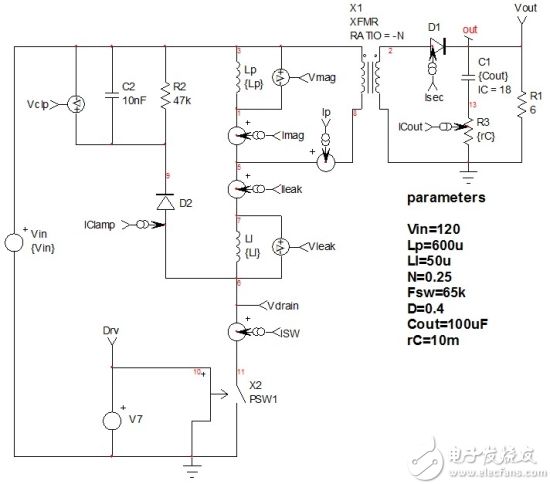
Figure 5: This simple model simulates a flyback converter and shows its basic waveform.
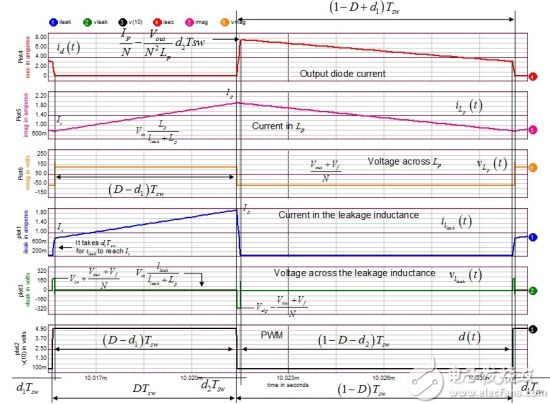
Figure 6: These waveforms show all the events we described above.
Through simulation, we can extract the following operating points, where Vclp is the voltage across C2:
Ip=1.77A
Iv=672mA
Vclp=528V
The leakage inductance magnetization time is as described in (14) and measured as 176 ns. Using 65-kHz switching frequency, duty cycle d1 is

(22) In theory, the transformer turns ratio N is 0.25, so the output voltage of the flyback converter is defined as (21) equal to 20V. If we use (20), the output voltage should actually be equal to

(23) The simulated output voltage is shown in Figure 7 and the value is determined. Note that the forward voltage drop of the diode we used in the simulation is 0 V. You can get this result by setting the diffusion parameter N to 10m in the diode model.
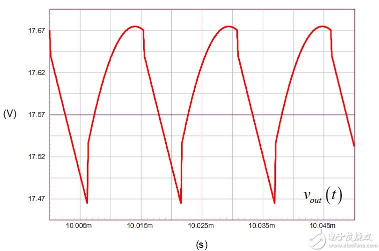
Figure 7: These waveforms show all the events we described above.
If you know the leakage inductor reset time, you can also accurately calculate the output current. The simulation provided a valley current of 672 mA and a peak current of 1.77 A. Application (16) and considering the 528 V clamping voltage (voltage across C2 in Figure 5), the leakage inductance reset time is
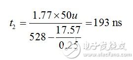
(24) The corresponding duty cycle is

(25) We can also estimate the secondary peak current when the leakage inductance is reset after 193 ns after the switch is turned off. Application (13), we found

(26) From the low-side waveform of Figure 3, we can now determine the average current circulating through the diode and load by calculating the various fields that make up the curve:

(27) import values, we have

(28) This is the value given by the waveform viewer, as shown in Figure 8.
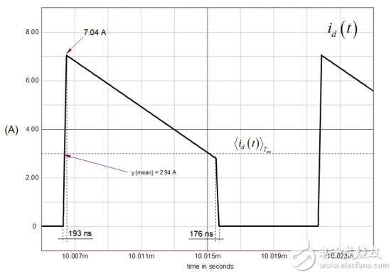
Figure 8: The simulated secondary-side average current is dependent on the peak and various small duty cycles d1 and d2.
Hardware verification
To confirm our analysis, we have established a simple fixed duty cycle flyback converter whose leakage inductance has been artificially increased to 2.5% of primary inductance by adding an external inductor. Figure 9 shows the MOSFET drain voltage and the secondary-side diode current. As expected, the secondary current did not increase immediately when the switch was turned on. This is the delay caused by the demagnetization time of the leakage inductance. On the right side of the diagram, you see that the diode waveform slightly lags behind the drastically decreasing drain voltage. This is the magnetizing time of the leakage inductance from 0 to the valley current. The close-up of Figure 10 confirms a turn-on time of 62 ns. The turn-on and fall-down vDS (t) of the MOSFET is well synchronized, but the Lp magnetization cycle really starts after 62 ns. During this 62 ns, Lp remains demagnetized although the MOSFET has turned on. This phenomenon is very short here, obviously negligible. However, you can clearly observe the delay, which will result in a significantly longer active clamp architecture.
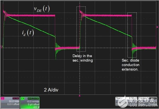
Figure 9: The acquired prototype waveform shows the secondary side delay, but the small secondary diode conduction time also increases.
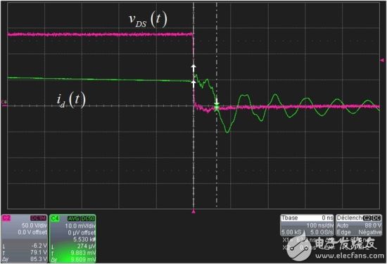
Figure 10: Close-up of falling edge shows secondary diode delay 62 ns
In Figure 11, you can clearly see the secondary side current delay, but you can also calculate the leakage inductor reset time. During this period, the drain voltage reaches a stable value after the switch is turned on. In this case it lasts 217 ns. Overshoot is important and depends on the forward transmission time of the clamp diode. It must be considered when evaluating the MOSFET drain-source breakdown voltage (BVDSS). When the RCD diode is blocked, high-frequency ringing involves leakage inductance, Clump. Damping these oscillations is sometimes necessary because they can seriously radiate and affect EMI signals. Make sure that the circuit involving the RCD clamp is very short and close to the transformer. Sequencing tens of ohms in series with a diode helps dampen these oscillations.

Figure 11: Observe the required information for the drain voltage display, especially the leakage inductor reset time.
In this oscilloscope shot, the delay lasts for a short time because the leakage inductance resets quickly. However, in active clamp converters, resonances involving lleak and Cclamp occur at turn-off, naturally extending the reset time. This resonance produces a smooth discontinuous waveform at the secondary even when operating in CCM mode.
in conclusion
This first part shows that the flyback converter waveform is affected by the leakage inductance. The effective duty cycle reduces the time required to energize the leakage inductance, while the demagnetization of the primary inductor extends for the same amount of time. The Dc converter function is affected and a new expression is derived. These events are tiny in flyback converters and it is hard to imagine connecting them with a well-coupled transformer. However, in an active clamp converter, this time may be significant. Our second part will focus on the small signal effect caused by leakage inductance.
A high-speed slip ring is an electromechanical device that allows electrical current to pass between a stationary and a rotating assembly. It is typically used in applications where the speed requirement exceeds that which is achievable with a standard slip ring. High-speed slip rings are available in a variety of sizes and configurations to meet the needs of most applications. They are commonly used in military, aerospace, and medical applications where speed and reliability are critical.
The speed is required to be at least tens of thousands of revolutions per minute, the structure of the Conductive Slip Ring directly determines the contact of high speed, as well as the size of impedance. High-speed slip ring materials have high wear resistance, high life characteristics, and multi-contact contact can ensure signal transmission and power reliability, with the development of science and technology, high-speed slip rings will be more and more widely used.
If you need to transfer large amounts of data or power between two stationary objects, a high-speed conductive slip ring is what you need. Traditional slip rings only offer a few thousand revolutions per minute (RPM), which is more than enough for most applications, but can be limiting in some circumstances. Some applications, like those found in the medical or military field, require speeds of tens of thousands of RPM in order to function properly. That's where our high-speed conductive slip ring comes in. With speeds up to a certain range, it can handle even the most demanding applications.
High Speed Slip Ring,Rotary Slip Ring Electrical,Slip Electrical Connector,Hydraulic Rotary Joint
Dongguan Oubaibo Technology Co., Ltd. , https://www.sliprobs.com