In a sodar system, the transmitter emits acoustic signals of different frequencies, and then receives echo signals at different distances. The deviation of the wind speed and the wind direction with height can be measured by the deviation of the frequency in the echo. The signal acquisition system based on American Analog Devices' DSP ADSP-TS201S and ADC AD7864 described in this paper can meet these requirements.
System design
1 system function module division
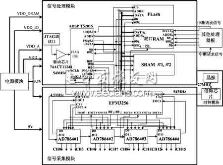
The sodar signal acquisition system is mainly composed of signal acquisition, signal processing, power supply and clock, as shown in Figure 1. The signal acquisition module consists of CPLD and 4 ADCs, which is responsible for A/D conversion; the converted data is sent to the signal processing module, DSP ADSP-TS201S is responsible for data reception and processing, and two 512k&TImes; 32b SRAMs complete multi-frame Data storage tasks; a dual-port RAM provides a convenient interface for ADSP-TS201S and other processor boards to exchange information, and Flash is used to store user applications. The power module provides the voltage required for normal operation of other modules. In the clock module, the 27MHz clock generated by the crystal oscillator enters the CPLD through the multiplier chip and obtains the 54MHz clock. It is used as the system clock SCLK of the ADSP-TS201S on the one hand, and as the working clock signal of the AD7864 on the other hand after dividing by 12 in the CPLD. AD_CLK.
The reason why the system uses ADSP-TS201S chip is derived from its powerful processing capability, and can process a large amount of echo data in real time. It can achieve 4.8 billion times of multiply-accumulate (MAC) operations and 3.6 billion floating-point operations per second (FLOP) at 600MHz core clock, which is 50% to 100% higher than comparable processors. It integrates 24Mb of internal memory, and this on-chip large amount of memory combined with up to 33.6Gb/s of internal bandwidth is the key to improved performance. Its external 64-bit data bus and 32-bit address bus clock can be up to 125MHz.

Figure 1 Circuit diagram of the signal acquisition system
In the sodar system, multi-channel simultaneous sampling is required. The high-speed multi-channel and simultaneous sampling characteristics of the AD7864 chip meet the requirements of the system and simplify the hardware design. Its conversion accuracy is 12 bits, and the throughput can reach up to 520KSPS. Single channel conversion time The fastest time is 1.65μs and the sample/hold time is 0.35μs. In addition, its single-supply and low-power features (up to 20μW) also meet system requirements.
When the system works, the back-end processor board first sends an interrupt signal to the ADSP-TS201S, informing the TS201 to read the command word from the dual-port RAM. According to the command word, TS201 controls the data of the front-end ADC through CPLD and uses DMA to read the data. The processed data is stored in the dual-port RAM. TS201 also informs the back-end processor board to read the data through the interrupt mode. display.
2 hardware circuit design
In the design of the clock circuit, the power supply of the crystal oscillator and the multiplier chip is isolated from the power supply of the board by an inductor or a magnetic bead to prevent coupling interference to the system power supply. In order to suppress current surge and low frequency interference caused by voltage fluctuations, a 10μF tantalum capacitor is added to the power supply pin, and a 0.1μF small capacitor for suppressing high frequency interference is also necessary. Place it close to the pin. In addition, care should be taken not to route the wires under the clock chip to prevent mutual coupling interference. A 33Ω matching resistor can be added to the output of the multiplier chip to reduce the output current and improve the quality of the clock waveform. To reduce EMI emissions and clock jitter, minimize the use of vias.

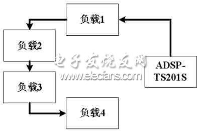
(a) Ring structure

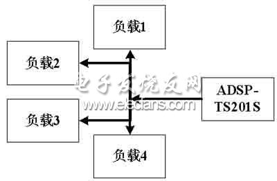
(b) star structure
The design of the bus at high frequencies also needs attention, especially in the case of heavy bus load in the system. Inappropriate design will limit the bus to work only at low frequencies or even read data. Since any load variation on the ring structure will affect the operation of other loads, a star bus structure is used in this design, as shown in Figure 2. Considering the driving ability of the DSP bus in the wiring process, the length of each signal line is strictly controlled to about 6 inches. Practice has proved that the above measures are necessary and correct.
The ADSP-TS201S and AD7864 have very high power requirements. For example, when the S201 requires a 500MHz core clock, its four power supplies VDD, VDD_A, VDD_IO, and VDD_DRAM have an accuracy of ±5%. Therefore, the output voltage accuracy is used in the system. Up to ±1% of the TPS54350 is used as a power chip.
The power consumption of the ADSP-TS201S can be calculated as follows. Taking 500MHz as an example, the current consumed by the VDD domain can reach 2.67A, which is available from equation (1). With the current of VDD_A, the maximum power consumption of the core is 2.99W.

From equation (2), the maximum power dissipation in the VDD_IO domain is 580mW.

According to equation (3), the maximum power consumption of the internal RAM is 600mW.

Based on the above data, from equation (4), the total power consumption of the ADSP-TS201S at 500MHz is 4.17W.
(4)

The power consumption of the ADSP-TS201S is still relatively large, so it is designed to make room for the heat sink or fan. The high frequency noise of the power supply part will affect the working speed of the ADSP-TS201S, especially the part with voltage less than 1.5V. Therefore, the low-ESR ceramic chip capacitor filter should be used near the power input pin of TS201, in addition to VREF and SCLK_VREF The foot also needs to pay attention to filtering.
Since the system is a digital-analog hybrid circuit including an ADC, the following issues should be noted in the design. A large area of ​​copper around the AD7864 and CPLD shields external analog signals, while the AD7864's power supply pin, reference voltage input pin, VDRIVE pin and analog ground are decoupled with a 0.1μF chip capacitor. Digital signal traces and analog signal traces should be placed separately; the digital ground and analog ground of the whole board should be separated and single point connected, and the connected points should be selected in the place where the analog signals are collected; the 5V power supply for the AD7864 needs Stay away from the AD7864.
During the debugging process, if the driver chip is not added to the JTAG port of the ADSP-TS201S, the Visual DSP will go wrong when cutting into the hardware emulation environment. Therefore, it is recommended to add a driver chip even for the single-chip ADSP-TS201 system, such as TI. 74ACT11244.
In order to improve the flexibility of the system, it is recommended to provide pull-up and pull-down options for the SCLKRAT0~2 (for selecting the multiplication factor) and DS0~2 (for selecting the bus drive capability) pins of the ADSP-TS201S. The actual situation in the flexible configuration.
The main control unit of the equipment is PLC and the HMI (Human Machine Interface) is 7" LCD colorful touch screen. The equipment has varieties of operating modes, and can automatically record and save working status.The complete set of equipment is easy to operate, reliable in working, complete in protection and high in automation.
It has the features of high reliability, high pulse symmetry, strong anti-interference ability, quick reaction, as well as the advantages of no heat-generating, constant current, energy-saving which is compared with the discharge with the electrical resistance.
Agv Battery Charger And Discharger
Battery Charger Discharger,Charging And Discharging Of Battery,Intelligent Battery Charger And Discharger,Agv Battery Charger And Discharger
Xinxiang Taihang Jiaxin Electric Tech Co., Ltd , https://www.chargers.be