In the traditional sense of the SiP system-in-package, anything that has a chip stack can be called 3D because there is a function and signal extension on the Z axis, whether the stack is inside the IC or outside the IC.
But at present, with the development of technology, 3D ICs have their newer and more unique meanings.
Chip-stacked 3D technology
The initial state of 3D ICs is still widely used in the field of SiP. The bare chips with the same function are piled up from the bottom to the top to form a 3D stack, which is then connected by bonding wires on both sides, and finally the system-level package (System). The appearance of -in-Package, SiP) is presented. The stacking method can be pyramidal, cantilevered, side-by-side stacking, etc. See the figure below.

Another common method is to mount a flip-chip bare chip on a SiP substrate, and another bare chip is mounted on top of it by bonding. As shown in the figure below, this 3D solution solves this problem. The program is more commonly used in mobile phones.

Passive TSV based 3D technology
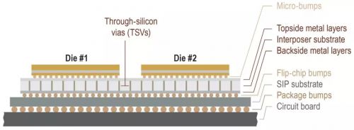
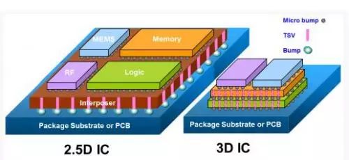
An interposer silicon substrate is placed between the SiP substrate and the bare chip, and the interposer is provided with through-silicon vias (TSVs), and the metal layers above and below the silicon substrate are connected through the TSV. Some people call this technique 2.5D, because the silicon substrate as an interposer is a passive passive element, and the TSV TSV does not hit the chip itself. As shown below:
Active TSV based 3D technology
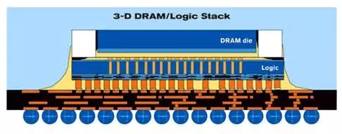
In this 3D integration technology, at least one bare chip and another bare chip are stacked together. The bare chip underneath is a TSV technology. Through the TSV, the upper bare chip communicates with the bare die and the SiP substrate below. . As shown below:
The figure below shows the 2.5D and 3D technologies for passive and active TSVs, respectively.
The above technologies all refer to stacking 3D after the chip process is completed. In fact, it cannot be called true 3D IC technology.
These methods are basically carried out in the packaging stage, we can call it 3D integration, 3D packaging or 3D SiP technology.
3D technology based on chip manufacturing
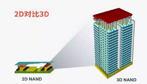
At present, 3D technology based on chip manufacturing is mainly applied to 3D NAND FLASH.
The pioneering work of Toshiba and Samsung on 3D NAND has brought two major 3D NAND technologies.
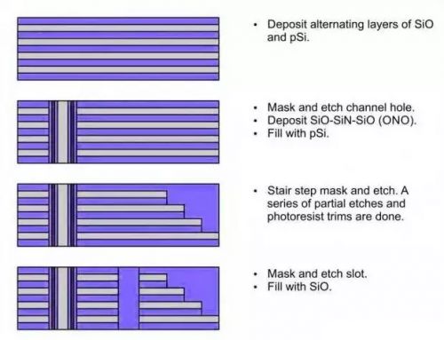
Toshiba developed the Bit Cost Scalable (BiCS) process. The BiCS process employs a gate-first approach, which is achieved by alternate deposition of oxide (SiO) and polysilicon (pSi) layers. A via hole is then formed in this layer stack and filled with oxide-nitride-oxide (ONO) and pSi. The photoresist is then deposited, and through a continuous etching process, the photoresist is trimmed and a step is etched to form the interconnect. Finally, a groove is etched and filled with oxide. As shown below.
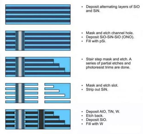
Samsung developed the Terabit Cell Array Transistor (TCAT) process. TCAT is a gate-last approach that deposits alternating oxide and nitride layers. A channel through these layers is then formed and filled with ONO and pSi. Then similar to the BiCS process to form a ladder. Finally, a trench is etched through these layers and nitrides are removed. Aluminum oxide (AlO), titanium nitride (TiN), and tungsten (W) are then etched back and etched back. Fill this slot. As shown below.
3D NAND can already achieve 64 layers or even higher, its output is exceeding 2D NAND, and as the number of layers is further expanded, 3D NAND can continue to keep Moore's Law well.
The 3D technology currently used in IC manufacturing is also limited to NAND FLASH. With the development of technology, it should soon be applied to other IC fields. At that time, the real 3D IC era is coming!
This scratch-resistant TPU Film protects your new AirTag from daily wear and tear. It can be easily glued to the back to keep the shiny silver in its original condition. In addition, the AirTag screen protector with "self-healing" function can automatically repair small scratches and bubbles within 24 hours. This means you can continuously enjoy the new look and appearance of AirTag without worrying about serious scratches and dents.
The Apple Airtag TPU Film can perfectly fit your AirTag skin. It is designed to provide the maximum coverage for your AirTag metal panels. Compatible with most AirTag shells. Leave extra space around the frame so that your shell can wrap the edges of the AirTag without interfering with the film.
The 0.14mm ultra-thin AirTag Screen Protector allows you to enjoy the maximum resolution while being thin enough to make the AirTag sensitive to the original signal response, ensuring that it will not affect any user experience. You won't even notice that the screen protector is there, so your Apple logo can still be displayed.
The AirTag Tracker Screen Protector is very easy to apply and is specially designed for your AirTag. Just clean your AirTag and install it on the surface to eliminate all bubbles and get the job done!
Apple Airtag Screen Protector, Apple Airtag Screen Protective Film, Apple Airtag TPU Film, AirTag Tracker Screen Protector, Skin Wrap
Shenzhen Jianjiantong Technology Co., Ltd. , https://www.hydrogelprotectivefilm.com