64 Kb/s A-law or μ-law logarithmic companding PCM coding has been widely used in large-capacity optical fiber communication systems and digital microwave systems, but it occupies a large transmission bandwidth and has a complicated framing structure. Continuously Variable Slope Delta (CVSD) modulation is widely used in tactical communication networks, satellite communications, Bluetooth and other wireless voice transmission fields due to its low application difficulty, cost and coding rate. Thus, the interconnection between networks of different code systems places higher demands on the conversion between the two code systems. In view of the continuous development of FPGA and DSP technology in recent years, this paper proposes a design scheme to meet this demand, in order to adapt to the rapid development of communication technology.
This article refers to the address: http://
1 multi-channel data signal transmission and reception
1.1 McASP (Multichannel Audio Serial Port)
McASP's new universal serial port for multi-channel audio applications based on the C5000 series of DSP processors, which includes two functions for receiving/transmitting, both of which can be fully synchronized or completely independent. The master clock, bit clock and frame sync clock have different data transmission modes and bit stream formats. Support multiple data protocols: I2S, S/PDIF, IEC60958-1, AES-3 and other format code streams, support time division multiplexing (TDM code stream), up to 32 channels for transceiving transmission can be 8 bits/ 12 bits / 16 bits 120 bits / 24 bits / 32 bits, etc.
1.2 Implementation of multi-channel data transmission and reception
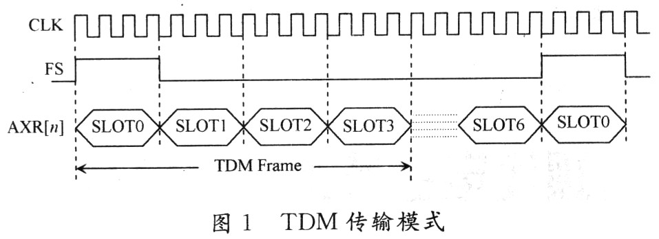
1.2.1 TDM Mode This article discusses the transmission of audio data. When MCASP works in TDM format, it can be used to directly connect DSP and multiple ADCs and DACs. The multiplexing of data depends on the transmission mode of up to 32 time slots per receive (transmit) frame. Figure 1 shows the transmission mode of six SLOTs.
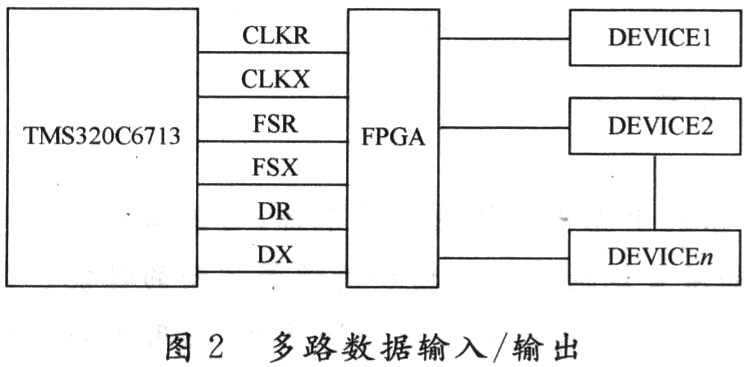
The TMS320C6713's multi-channel data output/input needs to go through a data combination and separate timing control unit. This task is completed by an FPGA. Its function is to receive all the data from the DSP and combine the same time slots according to the corresponding The timing of the connected devices is sent out, and the data from different devices are combined and sent to the DSP in TDM, as shown in FIG. 2 .
1.2.2 Clock and Frame Synchronization The specific mode of TDM can be set by setting the DSP's Transceiver Frame Synchronization Control Register. The corresponding bit clock and frame synchronization clock can be generated externally by program control or directly generated internally. Figure 3 is the clock. Related control relationships. The high frequency clock AHCLKX can be set to an internal or external input by the high frequency clock control register, and ACLKX can be set to an internal or external input by the clock control register. If the internal high frequency clock is used, it is obtained by dividing AUXCLK, and the frequency division value is determined by 0 to 11 b of the high frequency clock control register; the high frequency clock is divided to obtain the bit clock, and the frequency division value is determined by the clock control register. 0 to 4 b decision.

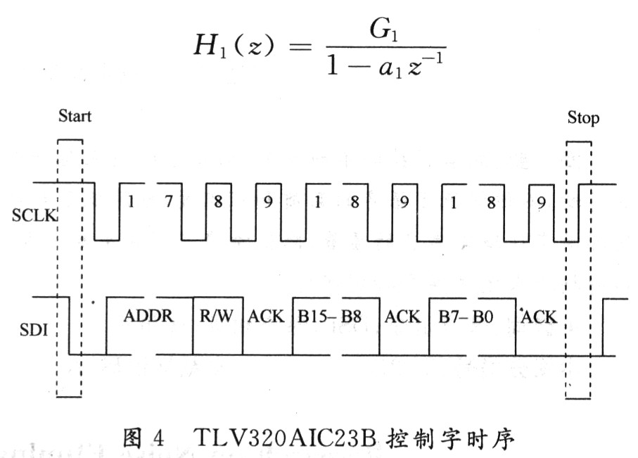
1.3 AD sampling and voice signal playback TLV320AIC23B is the input and output analog audio interface codec, the codec uses Sigma-Delta technology for digital-to-analog and analog-to-digital conversion, and directly connected to McBSP, AIC23 also provides a microphone Input, linear input, linear output and headphone output 4 analog interfaces. The control word of TLV320AIC23B can be written by SPI or I2C. Figure 4 is a read/write timing diagram of the I2C mode control word. After setting the working mode of the control register, the TLV320AIC23B can be used to accurately sample and play back the voice signal.
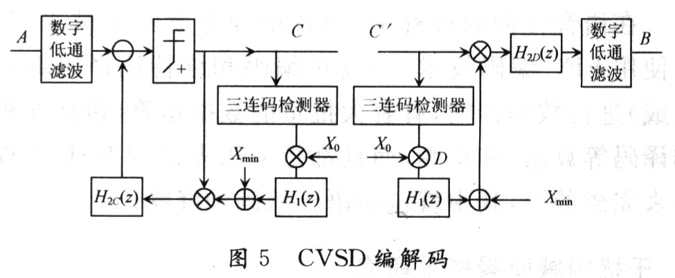
2 CVSD codec CVSD is also called digital detection syllable pressure amplification modulation, and has entered the practical stage for more than ten years. The transfer function of the main integrator in the syllable smoothing filter and the codec in the digital CVSD codec is as follows:
Syllable smoothing filter:
Encoder dual integrator:
Decoder main integrator:
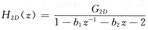
Figure 5 is a flow chart of the codec. By performing the inverse transformation of Z on the above formula, three difference equations can be obtained, and the corresponding codec code is written according to the corresponding difference equation.
3 PCM code and CVSD code conversion PcM code sampling frequency is 8 kHz, CVSD coded sampling frequency is 16 kHz, convert PCM code to CVSD code first convert PCM code into linear PCM, then add 2 times interpolation low pass The filter is used to convert the sampling frequency from 8 kHz to 16 kHz, and then sent to the CVSD encoder to generate a 16 Kb/s CVSD code; the conversion of the CVSD code into the PCM code is an opposite process, that is, the CVSD code is sent to the decoder. A linear PCM code is obtained, and the sampling frequency corresponding to the PCM code at this time is 16 kHz instead of 8 kHz. In order to convert the sampling frequency from 16 kHz to 8 kHz, a 2x decimation low-pass filter is needed to convert the linear PCM into an A-law PCM. The filter can choose the FIR filter.
4 Conclusion The input/output design of multi-channel audio data proposed in this paper utilizes the high-speed data processing function of 6000 series DSP, and simultaneously processes the CVSD codec of multiplexed data, the mutual conversion of PCM code and CVSD code, for different code system. The interconnection between networks has important application significance.
Low Frequency Inverter,Off Grid Solar System Inverter,Sine Wave Inverter With Charger,Off Grid Pure Sine Inverter
GuangZhou HanFong New Energy Technology Co. , Ltd. , https://www.hfsolarenergy.com