GMII, RGMII, SGMII, TBI, RTBI Interface Signals and Timing Introduction
There are five Gigabit Ethernet MII interface types: GMII, RGMII, SGMII, TBI, and RTBI.
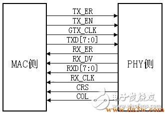
GMII connection (below): Compared with the MII interface, the GMII TX/RX data width is changed from 4 bits to 8 bits. The control signals in the GMII interface such as TX_ER, TX_EN, RX_ER, RX_DV, CRS, and COL have the same role as the MII. As in the interface, the frequency of the transmission reference clock GTX_CLK and the reception reference clock RX_CLK is 125 MHz (1000 Mbps/8=125 MHz). Here is a point that needs special explanation. It is to send the reference clock GTX_CLK, which is different from the TX_CLK in the MII interface. The TX_CLK in the MII interface is provided by the PHY chip to the MAC chip, and the GTX_CLK in the GMII interface is The MAC chip is provided to the PHY chip. The directions are different. In practical applications, most of the GMII interfaces are compatible with the MII interface. Therefore, the general GMII interface has two transmit reference clocks: TX_CLK and GTX_CLK (the directions of the two are different, as mentioned above). When used as MII mode, use TX_CLK and 4 of the 8 data lines. RGMII interface (as shown below):
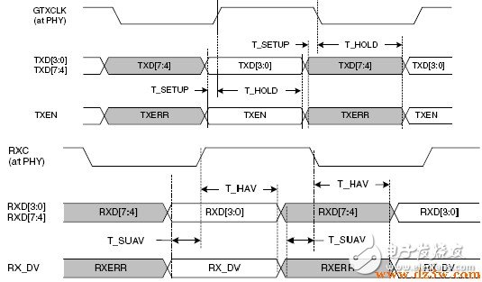
RGMII, Reduced GMII, is a simplified version of RGMII, reducing the number of interface signal lines from 24 to 14 (COL/CRS port status indication signals, not shown here), the clock frequency is still 125 MHz, and the TX/RX data width is from 8 is changed into 4 bits, in order to keep the transmission rate of 1000Mbps unchanged, the RGMII interface samples data at both the rising and falling edges of the clock. TXD[3:0]/RXD[3:0] in the GMII interface is transmitted on the rising edge of the reference clock, and TXD[7:4]/RXD[7:4] in the GMII interface is transmitted on the falling edge of the reference clock.
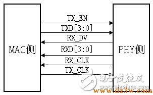
RGMI is also compatible with both 100Mbps and 10Mbps. The reference clock rates are 25MHz and 2.5MHz. TX_EN signal transmit TX_EN and TX_ER two kinds of information, in the TX_CLK rising edge to send TX_EN, falling edge to send TX_ER; Similarly, RX_DV signal line also transmits RX_DV and RX_ER two kinds of information, in the RX_CLK rising edge to send RX_DV, falling Send RX_ER along. RGMII transceiver timing as shown below:
SGMII interface (as shown below):
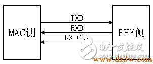
SGMII is Serial GMII, serial GMII, which transmits and receives each pair of differential signal lines. The clock frequency is 625MHz. It is sampled on the rising and falling edges of the clock signal. The reference clock RX_CLK is provided by the PHY and is optional. It is mainly used on the MAC side. In the absence of a clock, under normal circumstances, RX_CLK is not used. Both send and receive can recover the clock from the data. In the TXD transmit serial data, TX_EN/TX_ER two-bit control information is inserted for each 8-bit data. Likewise, in RXD receive data, RX_DV/RX_ER two-bit control information is inserted for each 8-bit data, so the total data rate is 1.25Gbps = 625Mbps * 2. In fact, most of the MAC chip SGMII interface can be configured as SerDes interface (physically compatible, just configure the register can be), directly external optical module, without PHY layer chip, At this time, the clock rate is still 625MHz, but at this time, unlike the SGMII interface, the SGMII interface rate is increased to 1.25Gbps due to the insertion of control information, and the rate of the SerDes port is increased due to the 8B/10B conversion, which was originally 8B/10B. The conversion is the operation of the PHY chip. In the SerDes interface, since the PHY chip is not connected outside, the 8B/10B conversion is completed in the MAC chip. The main role of the 8B/10B transformation is scrambling, so that the signal does not appear to be too long with "0" and even "1" conditions, affecting the extraction of clock information, on 8B/10B transformation knowledge.
TBI interface (as shown below):
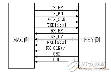
TBI means the Ten Bit Interface means that the interface data bit width is increased from 8 bits to 10 bits of the GMII interface. In fact, the difference between the TBI interface and the GMII interface is not very big. The extra 2-bit data is mainly because of the TBI interface. The MAC chip performs 8B/10B conversion before sending the data to the PHY chip (the 8B/10B conversion is done in the PHY chip, as already mentioned), and the RX_CLK+/- is recovered from the received data. Half-frequency clock, frequency is 62.5MHz, RX_CLK+/- is not differential signal, but two independent signals, there is phase difference of 180 degrees between them, sample the data on the rising edge of these two clocks. RX_CLK+/- is also called a pseudo differential signal. With the exception of what was said above, the rest of the signal is the same as in the GMII interface. The TBI interface of most chips is compatible with the GMII interface. When used as a TBI interface, CRS and COL are generally not used.
RTBI interface (as shown below):
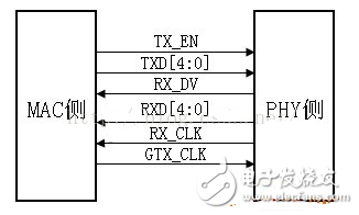
RTBI Reduced TBI, a simplified version of TBI, the interface data bit width is 5bit, the clock frequency is 125MHz, and the data is sampled on the rising and falling edges of the clock. Like the RGMII interface, TX_EN and TX_ER are transmitted on the TX_EN line. TX_EN is transmitted on the rising edge of the clock, TX_ER is transmitted on the falling edge, and RX_DV and RX_ER are transmitted on the RX_DV line. RX_DV is transmitted on the rising edge of RX_CLK, and RX_ER is transmitted on the falling edge.
Shenzhen ChengRong Technology Co.,Ltd. , https://www.laptopstandsupplier.com