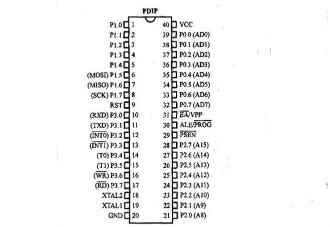
AT89S51 is a low-power, high-performance CMOS 8-bit single-chip microcomputer, which contains 4k Bytes ISP (In-system programmable) flash erasable 1000 times read-only program memory. The device uses ATMEL's high-density, non-easy The manufacturing of volatile memory technology is compatible with the standard MCS-51 instruction system and 80C51 pin structure. The chip integrates a general-purpose 8-bit central processing unit and ISP Flash memory unit. The AT89S51 is widely used in many embedded control application systems.
AT89S51 performance parameters1,4k Bytes Flash on-chip program memory;
2. 128 bytes of random access data memory (RAM);
3, 32 external bidirectional input/output (I/O) ports;
4, 2 interrupt priority, 2 interrupt interrupt nesting;
5, 5 interrupt sources;
6, 2 16-bit programmable timers/counters;
7, a full duplex serial communication port;
8, watchdog (WDT) circuit;
9, on-chip oscillator and clock circuit;
10ã€Compatible with MCS-51;
11, full static work: 0Hz-33MHz;
12, three-level program memory security lock;
13, programmable serial channel;
14, low-power idle and power-down mode.
AT89S51 pin and function
VCC: Supply voltage input.
GND: Power ground.
P0 port: P0 port is an 8-bit open-drain bidirectional I/O port. Each pin can absorb 8TTL gate current. When pin 1 of P1 is written for the first time, it is defined as a high-impedance input. P0 can be used for external program data memory. It can be defined as the lower eight bits of data/address. In FIASH programming, P0 port is used as the input port of the original code. When FIASH checks, P0 outputs the original code, and the external of P0 must be pulled high.
Port P1: Port 1 is an 8-bit bidirectional I/O port with internal pull-up resistors. Port 1 buffer can receive 4 TTL gate current. After P1 port pin is written to 1, it is internally pulled high and can be used as input. When P1 port is externally pulled down to low level, the current will be output because of internal pull-up. In FLASH programming and verification, P1 port receives as the lower eight address.
P2 port: P2 port is an 8-bit bidirectional I/O port with an internal pull-up resistor. P2 port buffer can receive and output 4 TTL gate currents. When P2 port is written “1â€, its pin is internal. The pull-up resistor pulls high and is used as input. Therefore, as an input, the pin of port P2 is pulled low externally and will output current. This is due to the internal pull-up. When the P2 port is used for accessing an external program memory or a 16-bit address external data memory, the P2 port outputs the upper eight bits of the address. When the address "1" is given, it uses the internal pull-up advantage. When reading and writing to the external eight-bit address data memory, the P2 port outputs the contents of its special function register. The P2 port receives high eight address signals and control signals during FLASH programming and verification.
P3 port: P3 port pin is 8 bidirectional I/O ports with internal pull-up resistor, which can receive 4 TTL gate currents. When P3 writes "1", they are internally pulled high and used as inputs. As input, because the external pull-down is low, the P3 output current (ILL) is due to the pull-up. In addition to being an ordinary I/O port, the P3 port has a second function:
P3.0 RXD (serial input port)
P3.1 TXD (serial output port)
P3.2 / INT0 (external interrupt 0)
P3.3 / INT1 (external interrupt 1)
P3.4 T0 (external count input of T0 timer)
P3.5 T1 (external count input of T1 timer)
P3.6 /WR (write strobe of external data memory)
P3.7 / RD (Read Gating of External Data Memory)
The P3 port receives some control signals for flash programming and programming verification at the same time.
When the I/O port is used as an input port, there are two methods of operation, the so-called read port and read pin. Reading the port does not actually read data from the outside, but instead reads the contents of the port latch into the internal bus and writes it back to the port latch after some sort of operation or conversion. Only when the port is read does external data actually read into the internal bus. The 89C51 P0, P1, P2, and P3 ports are quasi-bidirectional when used as input. In addition to P1, there are other functions of P0, P2, and P3.
RST: reset input, active high. When the oscillator resets the device, the RST pin must be held high for two machine cycles.
ALE/PROG: Address Latch Enable/Program Pulse Signal Terminal. When accessing external memory, the address latch allows the output level to be used to latch the lower byte of the address. During FLASH programming, this pin is used to input programming pulses. In peacetime, the ALE terminal outputs a positive pulse signal at a constant frequency, which is 1/6 of the oscillator frequency. Therefore it can be used as a pulse for external output or for timing purposes. However, it should be noted that each time an external data memory is used, an ALE pulse is skipped. To disable ALE output, set the SFR8EH address to 0. At this time, ALE only works when executing the MOVX, MOVC instruction. In addition, this pin is pulled slightly high. If the microprocessor is disabled in the external execution state ALE, the setting is invalid.
PSEN: External program memory strobe signal, active low. During the fetch from external program memory, /PSEN is active twice per machine cycle. However, these two valid /PSEN signals will not appear when accessing the external data memory.
EA/VPP: External program memory access allowed. When /EA is held low, external program memory (0000H-FFFFH) during this period, regardless of internal program memory. Note that with encryption mode 1, the /EA is internally locked to RESET; when the /EA pin is held high, the internal program memory is used. This pin is also used to apply the 12V programming power supply (VPP) during FLASH programming.
XTAL1: Input of the on-chip oscillator inverting amplifier and clock generator.
XTAL2: Output of the in-chip oscillator inverting amplifier.
Features of AT89S51 MCUAT89S5l is an upgraded product of AT89C51, and its performance is better. The AT89C51 has been greatly improved. It is similar to the AT89C51 in terms of price, and even lower.
The AT89S51 is distinguished by its addition of In-System Programming (ISP) functionality and no longer relying on dedicated programming tools. Rewriting programs in the microcontroller's memory eliminates the need to remove the chip from the board. AT89S series existing AT89S51/52/53/8252 and other members, the difference is that the built-in Flash memory and RAM capacity is not the same.
1, in the system programming ISP
From the pin, it can be seen that its P1.5, P1.6, and P1.7 are more multiplexed than the standard 8051. These three pins are used to implement the SPI in the system programming (ISP).
When the chip's RST pin is set high, all program and data memory can be programmed through the SPI bus interfaces MOSI (data input), MISO (data output), SCK (clock input) to the internal flash memory. A 3 MHz to 24 MHz crystal should be connected between XTAL1 and XTAL2 during programming, and the power supply voltage should be applied before VCC and GND.
Usually, the AT89S51 is connected to the PC parallel port (printing port) through the parallel port download line, and then Atmel's AT89ISP software can be used to program, verify, and encrypt (see the figure below).
2. On-chip watchdog timer WDT
The AT89S51 chip has a built-in 14-bit hardware watchdog timer WDT, which eliminates the need for external dedicated watchdog hardware. Once the WDT starts, there is no way to stop counting. Only hardware reset or overflow of the WDT can stop the WDT counting, which can effectively prevent the program from running and falling into an endless loop. Of course, without the built-in watchdog, the AT89S51 can be used exactly like an ordinary 8051 microcontroller.
3. Dual DPTR data pointer
The standard 8051 has only one 16-bit DPTR data pointer, so when performing operations such as copying data blocks, the source address pointer and the target address pointer must be temporarily stored, and programming can be very troublesome. There are two DPTR data pointers DPTR0/DPTR1 in AT89S5l, can choose conveniently when DPS bit (AUXR1.0) is set 0 to select DPTRO, set 1 to select DPTR1. By executing the INCAUXR1 instruction, DPS can be quickly switched without affecting the high bit of AUXR1. Usage is exactly the same with PHILIPS microcontroller.
4, improved power management
AT89S51 addition to the 8051 has a low-power idle mode (set IDL = 1) and power-down mode (set PD = 1), also increased the power-down mode of the interrupt recovery mode and power-on reset flag POF (PCON. 4). The POF is automatically set to "1" when the power is turned on and can be set to sleep by the software and is not affected by the reset.
5, stronger program confidentiality
The new three-level encryption algorithm, which makes decryption of the 89S series microcontrollers impossible, greatly enhances the confidentiality of the program, so that it can effectively protect the intellectual property from being infringed. six. The 89S52, 89S53 and 89S55 of other similar models AT89S series are compatible with 8052, the on-chip RAM is 256 bytes, more than Timer2 of 89S51, the on-chip Flash memory capacity is 8K, 12K and respectively. 20K bytes.
89S8252/89S8253 is also compatible with 8052, on-chip in addition to 8K/12K bytes of Flash program memory (erasable 1000 times), there are 2K bytes of data memory (erasable more than 100,000 times).
In addition, the corresponding AT89LS series is AT89S series low voltage series, AT89LS51 power supply voltage is 2.7V ~ 4.0V, operating frequency is 0 ~ 16MHz.
6, cost-effective
At present, AT89S51/52/55 offer is 5.2/6.5/10.5 yuan, respectively, have a higher cost, you can choose to use the appropriate model based on application needs.
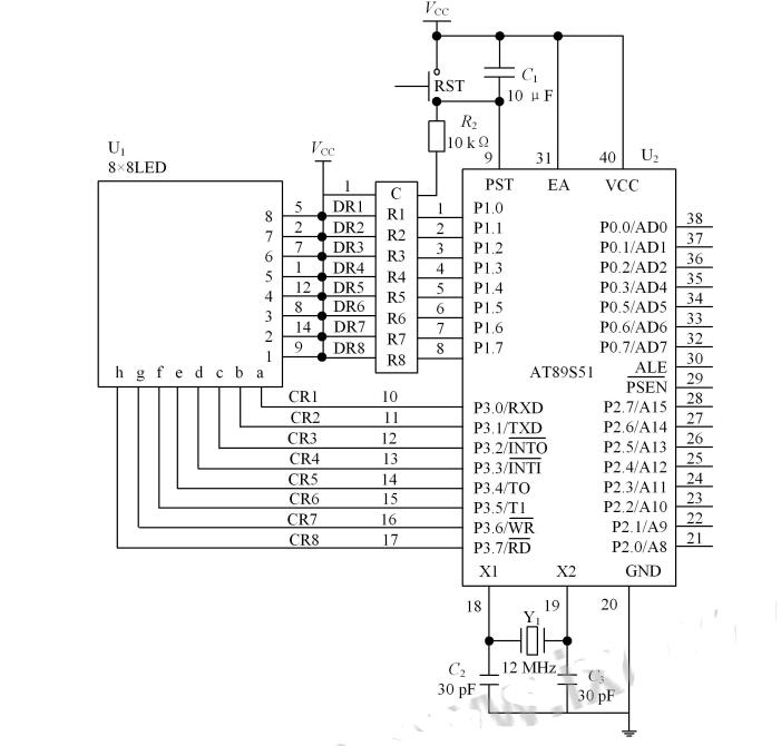
AT89S51 application circuitThe circuit in Figure 1 is a block diagram of an 8 × 8 dot matrix display circuit.

Figure 1
(1) Connect the P1 port in the "Single Chip System" area to the "DR1 to DR8" ports in the "Matrix Module" area with an 8-core core;
(2) Connect the P3 port in the "Single Chip System" area to the "DC1 to DC8" ports in the "Matrix module" area with an 8-core core; if you want to display a large image, multiple points can be put together The row and the row of the lattice are connected in series, and the columns and the columns are connected in series. A single row can be controlled with 74lS164.
High Power Eel Chip,Edge-Emitting Lasers Chip ,Edge Emitting Transistor Laser ,Edge Emitting Led Strip Light
AcePhotonics Co.,Ltd. , https://www.acephotonics.com