Abstract: In order to solve the conflict between high-speed digital image processing system and real-time, a real-time image processing system combining multi-DSP (digital signal processor TMS320C6416) and field programmable gate array (FPGA) is designed. The hardware resource selection, basic composition, working principle, power supply design, DSP guidance mode and software design of the system are introduced. The digital image processing results of 14 frames per second with 14 bits 640 & TImes; 512 pixels show that the system meets the high speed. The requirements for real-time image processing. At the same time, it can be extended to higher speed DSPs (such as the TMS320C6455 series) for more complex real-time image processing tasks.
With the rapid development of high-speed digital circuits, DSP chip integration, computing speed, data throughput and other performances continue to improve, DSP is no longer limited to traditional audio and video processing and offline signal processing applications, it has been widely used In many real-time video and signal processing transmission areas. In the real-time image processing system, how to complete the processing of a large amount of information data in a limited time, to meet the real-time requirements of the system has been a problem that plagues people [1]. Considering that a single DSP is difficult to meet the requirements of large amount of computation, high real-time performance and high data transmission rate in image processing, a real-time image processing system combining multiple TMS320C6416 as core processor and FPGA (Virtex-4) is designed. ]. The system can effectively combine the advantages of both DSP and FPGA, and preprocesses the image with FPGA, which greatly improves the flexibility of the system and provides a broad space and platform for the research and application of real-time image processing [3] ].
1 system hardware platform device selection 1.1 TMS320C6416 Introduction The core part of the system selects TI's TMS320C6416 DSP chip. This DSP has the following features:
1 8 Mbit on-chip memory 2 Extended direct memory access (EDMA)
3 host interface (HPI)
4 PCI interface 5 External memory interface EMIFA and EMIFB. Where EMIâƒ
FA bus width is 64 bit, EMIFB bus width is 16 bit
6 multi-channel buffer serial port (McBSP)
7 UTOPIA interface (ATM slave interface)
8 32-bit timer 9 16 general purpose I/O ports (GPIO)
Due to online image processing, image correction, and target recognition, the system has a large amount of computational data, and this chip provides high computational speed, large memory space, sufficient I/O interface, diverse communication methods, and wide range. The temperature of use provides sufficient time and space for the software design of the system, as well as the ability to adapt to harsh operating environments. In addition, the BGA package also provides protection for the system's anti-interference ability [4].
1.2 Virtex-4 Introduction System FPGA Select Xilinx's XC4VLX100-10FF1513 chip [5], this device has a wealth of logic resources to meet the design requirements. The Virtex-4 FPGA is the fourth generation Virtex family of FPGA products from Xilinx. Xilinx's Virtex-4 family combines the advanced silicon combination module (ASMBL) architecture with a wide range of flexible features to dramatically increase programmable logic design capabilities, making it a powerful alternative to ASIC technology. The product uses advanced deep sub-micron design technology, integrated hard IP blocks, and cubic 90 nm copper CMOS process technology, produced using 300 mm (12-inch) wafer technology, resulting in a 50% reduction in device cost and power consumption. The basic Virtex-4 building block is an enhanced version of the original building blocks (available in the popular Virtex, Virâƒtex-E, Virtex-II, Virtex-II Pro and Virtex-II Pro X product families), so the previous generation was designed Can be upward compatible.
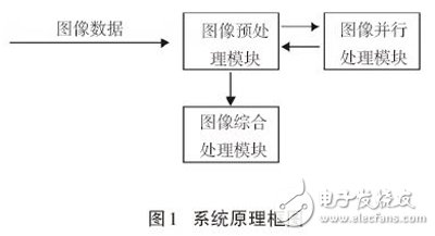
2 system designIt is mainly divided into three parts, namely image preprocessing module, image parallel processing module and image integrated processing module [6]. The system block diagram is shown in Figure 1.

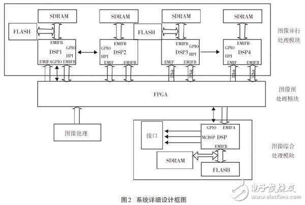
The detailed design block diagram of the system is shown in Figure 2.

2.1 The image preprocessing module uses Xilinx's Virtex-4 series chip and XCF32PVO48C series chip, which mainly realizes image data segmentation inside the FPGA and transmits the image to 4 DSPs (image parallel processing module) for parallel processing. DSP pair The received image is processed in real time and then transmitted to the DSP in the image synthesis processing module via the FPGA for comprehensive processing. 8 dual-port RAMs are customized in the FPGA, in which 4 pieces of DSP transmit image data, and 4 pieces of images are processed by the parallel processing module to the EMIFA interface of the image integrated processing module DSP.
2.2 Image parallel processing module uses TI's TMS320C6416 series DSP chip, AMD's AM29LV800A series FLASH chip and Miâƒ
The cron company's MT48LC16M16A2BG series SDRAM chip mainly completes the parallel processing of image data. There are four TI6416 DSPs on the signal parallel processing module, which are DSP1, DSP2, DSP3 and DSP4. Among them, only DSP1 and DSP3 have FLASH. Therefore, DSP1 needs DSP1 to boot DSP2 through HPI, and DSP3 boots DSP4 through HPI. Each DSP receives a 1/4 frame image. The DSP reads the image data from the FPGA through CE2 of EMIFA. After image processing, it writes four 256 Mb DPRAMs through EMIFB, and transmits the processed data to the FPGA through CE2 of EMIFB. GPIO1 of DSP1 is used to reset the FPGA. When GPIO1 is low, the FPGA is in the reset state, and when it is high, it is working. GPIO7 of DSP1, DSP2, DSP3, and GPIO5 of DSP4 are used to receive the signals of the FPGA. When the FPGA prepares the image data, the signals are pulled down for about 2ms to notify the DSP to read the image data. The GPIO15 of DSP4 is connected to the DSP of the signal synthesis processing module through the FPGA, and is used to notify the DSP to read the data processed by the signal parallel processing module.
2.3 The image synthesis processing module adopts a hardware platform similar to the image parallel processing module. The DSP reads the data processed by the signal parallel processing module through the EMIFA interface, and performs comprehensive processing on the data. The DSP connects a FLASH and SDRAM through EMIFB. After the image parallel processing module processes the data, the FPGA first sends a low level to the external interrupt pin GPIO5 of the image integrated processing module DSP, triggering the DSP external interrupt, and the DSP then uses the EMIFA CE0 to synthesize the SRAM from the FPGA. Read the data. DSP1 reserves 3 MCBSP channels to realize information communication between the image integrated processing module and the host computer such as PC.
2.4 Power Supply Design Due to the use of multiple types of integrated chips, such as FPGA and DSP itself are multi-voltage operation, the required operating voltage is 3.3, 2.5, 1.8, 1.25, 1.2 V and so on. Using TI's TPS54310 switching voltage conversion chip, the voltage value required for output is realized by externally connecting different resistors and capacitors.
2.5 DSP program guide
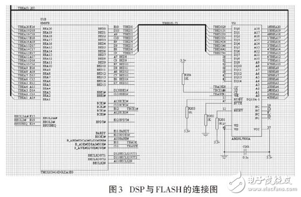
(1) The DSP, DSP3 and DSP of the image processing module of the FLASH boot image parallel processing module are guided in this way. The boot mode is booted from 8-bit FLASH (Bootmode [1:0]=10), and the FLASH capacity is 1 M×8 bit, and the fastest read/write period is 90 ns. Figure 3 shows the connection diagram between DSP and FLASH [7]. The EMIFB of the DSP is connected to the FLASH according to the asynchronous access mode, and the 1 M byte of the FLASH corresponds to the 0×64 000 000-0×64 100 000 (EMIFB CE1) addressing space of the DSP. FLASH works in 8-bit mode.

After the DSP power-on reset, the CPU automatically copies the first 1 Kbyte data (0×640 00 000-0×64 000400) of the CE1 interval of EMIFB to the internal RAM (0×00 000 000- 0×00 000400). Perform a boot (the copied code consists of two parts: the interrupt vector table (0 × 64 000 000 - 0 × 64 000 200) and the secondary bootloader program, which should be burned into FLASH beforehand). Then the CPU generates a reset interrupt, the program pointer points to the address 0×00 000000, and the program pointer points to the beginning of the secondary boot loader after the jump instruction is executed. The secondary bootloader implements the function of copying the entire application (which has been burned into FLASH beforehand) to its running address (internal RAM, so that the program runs fastest) and performs a second boot. At the end of the secondary bootloader program is a jump instruction, the CPU jumps to _c_int00 and begins executing the application [8].
(2) The DSP2 and DSP4 of the HPI boot image parallel processing module are booted by the HPI mode, and the DSP2 boots the program by the DSP1 through the HPI interface. The DSP1/DSP2 programs are stored in the off-chip FLASH of DSP1. After the DSP1 is powered up and the program is booted, the DSP1 program pointer jumps to the start address of the DSP1 application code to start executing the program. The DSP1 application first resets the DSP2; then reads the DSP2 program code from the FLASH, writes the corresponding address space in the memory of the DSP2 through the HPI interface; finally, the DSP1 wakes up the DSP2 through the HPI interface, and completes the program guidance to them [9].
Ebang Ebit Mining Machine:Ebang Ebit E11++,Ebang Ebit E9,Ebang Ebit E9.2,Ebang Ebit E9+,Ebang Ebit E9i,Ebang Ebit E11+,bang Ebit E10,Ebang Ebit E11
Ebang is a blockchain production company specializing in the production of Bitcoin machines. Their ebit series has always been a cost-effective series of Bitcoin machines, with stable income, low machine loss and guaranteed after-sales service.
Ebang Ebit Mining Machine,E9 25Th/S Miner,ebit miner,ebit mining machine,ebang miner
Shenzhen YLHM Technology Co., Ltd. , https://www.ylhm-tech.com