Abstract: In order to change the current situation of CPU resource utilization and keyboard shortage caused by CPU control matrix keyboard, an FPGA-based matrix keyboard controller is introduced. In the ISE13.4 development environment, a data error caused by the vibration of the mechanical matrix keyboard keys is developed using the VHDL hardware language; the functions of automatic scanning, encoding, storage, and output of the matrix keyboard are realized; The data is sequentially displayed on a matrix of eight 7-segment digital tube controllers. The designed VHDL controller was configured on the developed hardware circuit system to verify the correctness of each function design.
In the portable electronic equipment, there is a widely used matrix keyboard, which is generally scanned and controlled by a single-chip microcomputer, which greatly reduces the ability of the single-chip microcomputer to process other information, resulting in waste of resources. Using FPGA's powerful logic processing capability and rich pins, this paper designs an FPGA-based matrix keyboard controller, which mainly includes matrix keyboard anti-jitter module, scanning module, decoding module, storage module and digital tube display module. The data entered by the keyboard is displayed by a 7-segment digital tube.
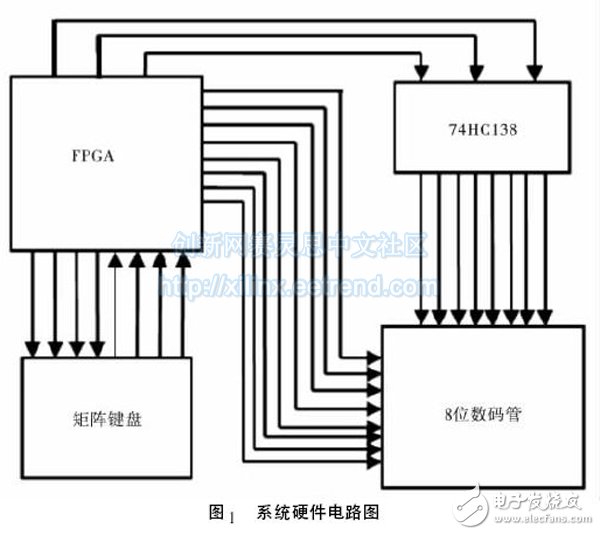
1 matrix keyboard controller and display circuit design ideasIn order to complete the human-computer interaction of the portable device, the FPGA-based matrix keyboard controller and display circuit are designed by using 4 &TImes; 4 matrix keyboard, as shown in Figure 1. The system is mainly composed of FPGA, matrix keyboard, 138 decoding chip and digital tube. It mainly completes an 8-digit input and stores the input 8 digits for subsequent use. The display function of the digital tube is used to confirm the input. Whether the data is accurate and reduces input errors.
It can be seen from Fig. 1 that the software part of the system mainly implements matrix keyboard row and column scanning control, input anti-shake, button decoding, button storage and digital tube display.
(1) Matrix keyboard row and column scanning control module: Generate periodic scanning signal, judge whether there is a button pressed according to the scanning input signal, if the button is pressed, immediately perform button judgment and encoding, and store the button to the inside register.
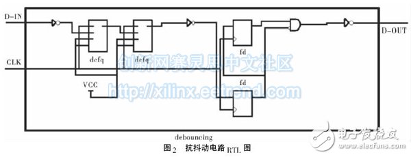
(2) Bounce elimination circuit: The matrix keyboard of the mechanical switch structure, when the button is pressed, the contact point will bounce back and forth. During the signal bounce time, the program cannot effectively judge the key value, which affects the correctness of the input and reduces the performance of the device.
(3) Key decoding circuit: Scanning the reply signal (the signal input to the FPGA by the button) can not be directly used as the subsequent signal in the FPGA. The intermediate signal must be defined to distinguish the functions of different buttons and decode the button.
(4) Key storage circuit: The input data of the previous key will be overwritten by the new key data generated by the next scan, so a shift register is needed to save the input of the entire key.
(5) Digital tube display circuit: In order to complete the input display of 8-bit data, it is necessary to scan and control each digital tube, and decode and display the digital tube according to the key value.

The matrix keyboard anti-jitter circuit mainly has four methods of counter, shift register, D-type flip-flop delay and sampling type anti-shake differential circuit [2]. The debounce method used in this paper is as follows: The keyboard input signal is used as the circuit input signal. Under the action of the clock signal, the input signal is delayed by the two-stage D flip-flop and then processed by the RS flip-flop. The frequency of the pulse signal used by the jitter elimination circuit must be higher than the frequency of the pulse signal used by other circuits. Usually, the operating frequency of the scanning circuit is set at about 24 Hz, and the operating frequency of the bounce circuit is set at about 128 Hz [3]. According to the above design ideas, the keyboard anti-jitter module is written in VHDL hardware language. The RTL circuit diagram of the anti-jitter module is shown in Figure 2.

The clock circuit mainly generates the clock signal required by the system, and the system clock is divided by the FPGA clock, and then the counter frequency division method is used to obtain the required bounce cancellation clock signal, the keyboard scan signal, and the digital tube display clock signal. The keyboard scanning circuit is used to generate a keyboard scanning signal. According to the working principle of the matrix keyboard, it is necessary to generate periodic scanning signals from the first column to the fourth column. The scanning module is designed in VHDL hardware language. The specific procedure is as follows.

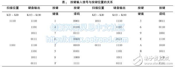
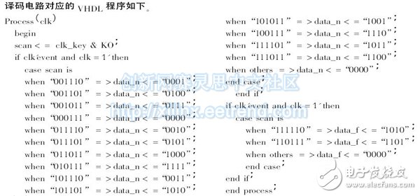
The scan reply signal generated by the matrix keyboard (the signal input to the FPGA by the button) cannot be directly used as a signal inside the FPGA. Before use, the scan reply signal needs to be decoded into a BCD that can be recognized by the FPGA according to different functions defined. Encoding, complete the decoding of the matrix keyboard input, and distinguish the functions of different buttons. The main functions of the decoding circuit are: judging whether a key is pressed, and then confirming whether the pressed key is a numeric key or a function key according to the scanned signal, and writing the pressed key into a BCD code. Table 1 shows the relationship between the keyboard input signal and the button position.


Each scan produces a new key input that may overwrite the previous data, so a key memory circuit is required to record the results of the entire keyboard scan. The key storage circuit is composed of a shift register circuit. This design uses a serial input, serial output shift register as a key storage circuit. Design idea: The octal counter cnt is counted according to the appropriate frequency; for each number, a different value is assigned to the bit selection signal segweixh, and the value of segweixh is output to the 138 decoder through the I/O port; When segweixh changes, the four bits of the keyboard input signal are assigned to the internal register datebuf according to a certain algorithm; the process (datebuf) process is the digital tube display decoding stage, mainly completing the decoding of the input signal. (limited to length, slightly omitted)
3 Analysis of experimental results(1) Scanning circuit simulation analysis: Figure 3 shows the crossover and keyboard scanning simulation diagram, where clk is the FPGA clock signal with a frequency of 50MHz; clk_1kHz is the 1kHz keyboard scan working clock signal obtained by the 50,000 division; The keyboard is scanned by the internal frequency divider of the program, and clk_scan is the keyboard scanning signal. It can be seen from Fig. 3 that the simulation results are consistent with the theoretical requirements.

(2) Digital tube display circuit simulation analysis: Figure 4 shows the digital tube display simulation waveform, where clk is the FPGA with frequency of 50Mhz
Clock signal; clk_1khz displays the working clock signal for the 1khz digital tube obtained by dividing by 50,000; the matrix keyboard input data is stored in the shift register datain_x, assuming the input data is "0000 0001 0010 0011 0100 0101 0110 0111", the corresponding display The number is 0, 1, 2, 3, 4, 5, 6, 7; led_out is 138-bit selection signal, which is consistent with the theoretical value by simulation results; segma_out shows the broken code for the digital tube, which is available from Figure 4. When the led_out is "000", "001", "010", "011", "100", "101", "110", "111", "11111010", "00100010", "10111001", " 10101011", "01100011", "11001011", "11011011", "10100010", that is, 0, 1, 2, 3, 4, 5, 6, and 7 are consistent with the input data.

The matrix keyboard controller and its display circuit of this design are in ISE13. 4 After the simulation verification in the development environment, the hardware verification was carried out in a hardware system developed by using 138 decoder chip, matrix keyboard, FPGA and 4-bit digital tube. The hardware uses Xilinx series spartan-xc3s500E chip as the core chip. The experiment proves that the designed system can accurately accomplish the target function, and the hardware system results are consistent with the simulation results, which verifies the correctness of the system. The designed system has a low probability of misjudgment and a fast response speed, which can meet the design requirements. The module outputs the key code output by the button release control. Before the button is pressed for a period of time until the release button is pressed, the key value of the button cannot be continuously output at a certain interval, and the matrix keyboard has no continuous button function.
Imported Stainless Steel Wire,Stainless Steel Straight Wire,Soft Reinforcement Stainless Steel Binding Wire,Bright Surface Stainless Steel Wire
ShenZhen Haofa Metal Precision Parts Technology Co., Ltd. , https://www.haofametals.com