The analog-to-digital conversion digitizes the analog signal to obtain a discrete digital quantity approximate to the original signal, and quantizes the original signal by digital signal in bit-bit unit coding. This quantization is currently implemented by the hardware of the ADC (Analog-to-Digital Conversion) chip. The control of the chip can be done in three different ways according to system specialization through DSP (digital signal processor), ASIC (application specific integrated circuit) and FPGA (field programmable gate array). [2] The FPGA method is suitable for the programmable environment with high rate requirements. This design uses Xilinx Spartan3E FPGA to control and complete the analog-to-digital conversion function of TI's ADS1256 chip.
ADS1256 chip introductionThe ADS1256 chip is a high speed, low noise 24-bit analog-to-digital (A/D) converter that provides a complete high resolution analog signal measurement solution. The ADS1256 has a filter-stable buffer and a programmable gain amplifier to further reduce signal noise. The signal sampling rate is up to 30Ksps to meet sanitary and phytosanitary standards. In terms of external interface, the ADS1256 has an SPI-compatible 5V serial interface. The input voltage of the analog signal is 5V, and the output voltage of the digital signal is 1.8V~3.6V. The power consumption is 38mW in the standard operating mode and 0.4mW in the standby mode.
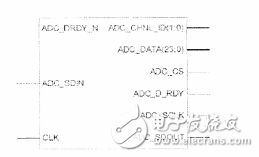
Overall and interface designThe input and output interface of the control system completed by FPGA is shown in Figure 3. One end can be connected to the ADS1256 chip, and the other end can combine the digital signals output by the chip into 24-bit precision data to connect the other data that the designer needs. Device.

(1) CLK: Connect the external 20MHz system main clock to drive the main control FPGA;
(2) ADC_DRDY_N: A/D data conversion ready signal, connected to the /DRDY pin of ADS1256, used to inform the master FPGA that the current analog-to-digital conversion is completed;
(3) ADC_SDIN: SPI serial data output signal of the main control FPGA, connected to the DIN pin of ADS1256, configure ADS1256 chip register; (4) ADC_CHNL_ID (1:0): input channel of digital signal after A/D conversion Connect D0 and D1 of ADS1256.
Output:(1) ADC_CS: The enable signal of the chip of ADS1256 is connected to the /CS pin of ADS1256;
(2) ADC_DATA (23:0): is the parallel output pin of the final data, can be connected to other required devices;
(3) ADC_D_RDY: used in conjunction with ADC_DATA to indicate that ADC_DATA is valid; (5) ADC_SCLK: SPI clock divided by the system main clock CLK, connected to the SCLK of ADS1256;
(4) ADC_SDOUT: The SPI serial data input signal of the master FPGA is connected to the DOUT of the ADS1256.
Function realizationThe overall module design should include the following sub-function modules:
(1) The clock module “clk_gen†divides the 20MHz main clock to generate a 2MHz clock with a 50% duty cycle and a 4MHz clock for the SPI; (2) The delay module “delay_n†is delayed for a period of time after the system is powered on. After waiting for the power supply to stabilize, initialize the A/D to start A/D conversion, reduce the instantaneous influence on the analog signal input when the system is powered on, and ensure stable data output during ADC conversion;
(3) Initialize the module "adc_iniTIal", its function is to initialize the ADS1256 through the SPI interface, and set it to work according to the instructions of the chip;
(4) AD conversion control module "adc_xchange", its function is to generate the timing required by ADS1256, send the control word to ADS1256 through SPI, and finally read the A/D converted digital signal according to the chip indication.
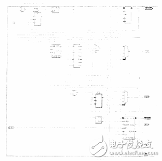
The RTL structure of the ADS1256 chip control system completed on the FPGA is shown below:

The system uses the 16-bit shift register formed by the Xilinx primitive SRL16E for clock control, which can be calculated by the following formula:
The number of data output bits = 8 * A3 + 4 * A2 + 2 * A1 + 1 * A0 + 1 For example, the system uses 20Mhz system main clock, to divide by 5 to get 4M SPI interface working clock, just A3, A2, D1, D0 can be set to 0, 1, 0, 0 (8 * 0 + 4 * 1 + 2 * 0 + 1 * 0 + 1 = 5).
The use of SRL16E in this design without the use of a latch (PLL) for clock division can further save FPGA hardware resources.
Because each lookup table LUT in the FPGA can form a 16-bit shift register, it can be implemented by calling the system macro SRL16E defined by Xilinx. A 16-bit synchronous RAM can be provided in the LUT. The recursive delay line (RDL) is designed by using the storage capacity of the SRL16E, and then combined with the time division multiplexing technique according to the multiplication of the RDL sampling rate and the time division multiplexing technique to form a recursive folding structure. Finally, at the cost of increasing the frequency of the main operating clock, the sampling rate and the throughput of the associated arithmetic unit are increased, and the use of resources is greatly reduced.
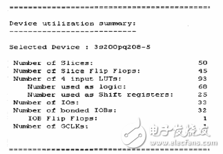
In this design, a 1/4 recursive folding structure is adopted, and the resource consumption is only 1/3 of that before optimization. As shown in the figure below, it is the resource usage of the FPGA.

FPGA resource usage.
Stainless Steel Round Bar,304 Stainless Steel Round Bar,Stainless Steel Flat Bar,Stainless Steel Threaded Rod
ShenZhen Haofa Metal Precision Parts Technology Co., Ltd. , https://www.haofametal.com