Abstract: A data acquisition system based on FPGA and ARM chip is designed. The FPGA is responsible for controlling the A/D converter to ensure the sampling precision and processing speed. ARM is responsible for the logic control and interaction with the host computer, and passes the collected data. USB is uploaded to the host at high speed for real-time processing. The test results of the analog data acquisition achieved high sampling accuracy and speed, which verified the high speed and feasibility of the whole system.
With the development of computer technology and modern industrial systems, the industry has put more stringent requirements on the accuracy of data acquisition and the real-time performance of data processing to ensure more complicated control. The traditional data acquisition system generally adopts A/. The method of matching the D chip with the main control chip has a slow processing speed and a single function. When the object to be measured is complex and the amount of data is large, it is difficult to satisfy the high-precision sampling of the data, and communication with the host computer through the RS232 serial port is even less. Guarantee the real-time nature of data processing. In response to this actual situation, a data acquisition system based on FPGA and ARM is designed. The FPGA is responsible for ensuring the high precision and high speed of data sampling. ARM is used as the main control chip and embedded in the Linux kernel. It is responsible for controlling the whole system and passing the data. USB high-speed upload to the host computer, with the powerful computing power of the host computer, to ensure the real-time data processing, and at the same time, according to different measured signals, only need to select the corresponding data acquisition card, you can easily and easily form a user-defined Data acquisition system with good versatility.
1 overall system designThe overall structure of the data acquisition system is shown in Figure 1. It consists mainly of input conditioning circuit, A/D conversion circuit, FPGA and ARM control circuit. The acquired analog signal is input to the A/D conversion chip via the conditioning circuit, and is analog-to-digital converted. It is sent to the FIFO memory module embedded in the FPGA under the control of the FPGA and notifies the ARM to immediately take the data, and finally delivers it via USB. The host computer performs real-time processing.

FPGAs have the advantages of high integration, high reliability, low power consumption and precise timing control. The Xilinx Spartan3 series XC3S200 is used to control A/D conversion and data buffering, which simplifies circuit design and shortens development cycle. ARM selects Atmel's SAM9G45 chip and operates at 400MHz, which ensures real-time high-speed control of the acquisition system and uploading data.
2. 1 FPGA and ADC connection and control data acquisition chip selects AD7656 of Analog Devices, which is a six-channel 16-bit successive approximation type, low power consumption, A/D conversion chip with maximum acquisition speed of 250kS /s per channel. Achieve higher sampling accuracy and speed.
The connection between FPGA and AD7656 is shown in Figure 2. The six sampling channels of AD7656 are divided into three groups. The corresponding two-channel synchronous sampling is started by three signals of CONV STA, CONV STB and CONV STC. The three pins are connected. Simultaneous sampling of 6 input channels is possible, and both parallel and serial interfaces are available. To improve data throughput, a 16-bit (/B pin low) parallel interface (SER/pin low) is used. Mode to transfer data directly to the 16-bit data line of the FPGA.
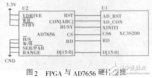
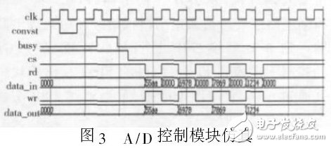
The A/D control module in the FPGA starts the sampling of the corresponding channel by pulling the CONV ST pin high. During the sampling process, the BUSY pin is high, indicating that sampling is in progress. When the sampling is completed, the AD7656 will automatically BUSY. Deassert; The A/D control block in the FPGA detects that the BUSY signal is low and then deasserts the CS and RD signals, reading and saving the data into the FIFO inside the FPGA. The FPGA simulation process for the AD7656 is shown in Figure 3.
2. 2 FPGA and ARM connection
The connection between FPGA and ARM is shown in Figure 4. In the communication with ARM, because it is cross-clock domain communication, in order to avoid metastable state, sample loss and potential logic errors, pulse edge detection method is adopted for ARM. The incoming control signal is first synchronized with the internal clock and then processed.
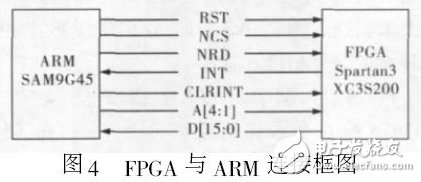
After receiving the ARM RST command, the FPGA controls the AD chip to start sampling. After detecting that the BUSY pin is low, the FPGA takes the data and buffers it into the FIFO, then changes the level on the INT pin to generate an interrupt to the ARM. Determining an interrupt, giving FPGA feedback through CLRINT, the FPGA will no longer generate an interrupt during CLRINT validity; ARM enables NCS and NRD signals to completely remove the data through data line D[15: 0], clear CLRINT signal, so that The FPGA can continue to generate interrupts to ARM.
The state transition process of the FPGA Interrupt Control Block is shown in Figure 5. When the BUSY signal is low and the data has been buffered into the FIFO, the INT pin is asserted to generate an interrupt and a timer is started. If CLRINT is valid during the timing period, the ARM is normally responded to the interrupt; if CLRINT is not valid until the end of the timer, the ARM is not detected to be interrupted or cannot respond normally, and the FPGA waits for a short period of time to generate an interrupt again.
 3 ARM system design
 ARM chip embedded in Linux 3. 0. The 4 version of the kernel, through the development of device drivers, enables stable and high-speed processing of FPGA data and real-time upload to the host via USB.
3. 1 FPGA driver
The FPGA driver is primarily responsible for controlling and reading the FPGA data and caching the data into structures such as KFIFO:
a. Manage the RST signal lines and control the FPGA for sampling.
b. According to the hardware circuit call, the specified area memory is requested for the FPGA. Since the chip has the MMU unit and cannot directly access the applied physical memory, the requested memory area needs to be remapped to the virtual address. When a read access is made to this memory area, the NCS and NRD signals are asserted by the core to be active low.
c. Request an interrupt line for the INT signal and register the interrupt handling routine. After the interrupt occurs, CLRINT is asserted high and the data is read from the mapped virtual address and saved in the KFIFO.
d. Re-enable the interrupt line and wait for the next interrupt.
The KFIFO is a first-in, first-out queue provided by the Linux kernel that caches data quickly and steadily. The FPGA driver exports the KFIFO symbol so that the USB driver can also access it directly and upload it to the host.
3. 2 USB driver
The Linux kernel provides a USB Gadget framework for USB device-side drivers, providing a good upper-level interface that hides the implementation of the underlying USB specification. The USB driver on the device side needs to provide a read endpoint 0x01 to read the control information of the host computer; write endpoint 0x82, report the status of the current acquisition system to the upper computer; write endpoint 0x83 to upload the collected data to the host computer. The main implementation process is as follows:
a. Configure 3 USB endpoint descriptors (one read endpoint 0x01, two write endpoints 0x82 and 0x83).
b. After receiving the sampling command of the host computer from the 0x01 endpoint, the initialization work is performed to notify the FPGA to start sampling.
c. Allocate memory for the request structure and copy the sampled data of the KFIFO buffer into the request package. The request structure is similar to the URB (USB Request Block) request package under Windows.
d. A write request is submitted to the 0x83 endpoint, and the data in the request packet is uploaded to the host via USB.
e. If an error occurs during the sampling process, such as a buffer overflow, report it to the host computer through the 0x82 port and request a restart.
The host computer USB driver uses the Driver Studio tool and Visual Studio 2010 as the auxiliary development environment. The host computer only needs to configure the same USB endpoint with the data acquisition device, send control commands to the ARM through the 0x01 port, read the status information of the acquisition system from the 0x82 port, and buffer the data received from the 0x83 port after the data processing program is read by the upper layer data processing program. take.
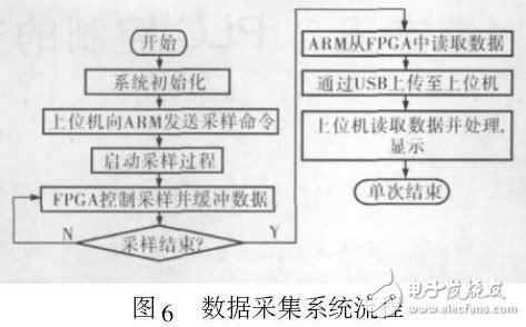
4 system overall process and experimentThe workflow of the acquisition system is shown in Figure 6. After the system is powered on, ARM boots Linux boot, initializes the internal registers and the RAM on the board, loads the USB driver and FPGA driver to the kernel, initializes the FPGA and configures the AD7656 working mode. After the initialization is completed and the host sampling command is received, the A/D starts sampling and the system enters the wait data state. After the sampling ends, the BUSY pin is pulled low to trigger the FPGA to notify the ARM to read the data. ARM quickly uploads the data and system status information from the FPGA to the host computer via USB. The host computer performs data processing operations according to the specific application to complete a collection.
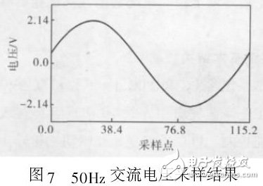
In the actual test, the AD7656 needs 3μs for each 6-channel acquisition and conversion. The actual working clock frequency of the FPGA is 40MHz. The main clock frequency (MCK) of the ARM is 133MHz, so the time required for data to be uploaded from the FPGA to the host is less than 1μs. That is, one sampling can be completed within 4μs, which satisfies the requirement that the system samples 256 times per cycle. The 50 Hz AC signal is sampled at 128 points per cycle. The sampling result is shown in Figure 7.
5 Conclusion Using FPGA + ARM chip combination data acquisition system, FPGA is responsible for sampling control, ARM is responsible for the logic control of the entire system, uploading to the host computer processing through the USB bus. The whole system has high sampling precision and fast data transmission, which can meet the complex requirements of multi-channel, high-precision, high-speed, real-time processing and easy manipulation in modern industrial systems. With the help of the Linux kernel, it can be easily implemented for different applications in different fields. The second development will have broad application prospects.
CKB currency is the brand new upgrade of this small mining coin in the sales market in 2020. The first mining machine to release this currency is developed by Toddminer, a team of ToddMiner. They became interested in the new Nervos project in early 2019, and immediately invested their scientific research energy when the Nervos team released CKB's Eaglesong optimization algorithm. After 2 years, ibelink finally developed a 32T KDA machine emperor, and the price is affordable compared with KD6, cost-effective and stable pressure tube over KD6 head, and there are two ways to convert freely, emerald green way calculation rate is only 22T, but the function loss is reduced to 1850w, customers can choose the different way according to their own situation. As a new star in the mining circle, iBelink company's new implementation of BM-K1,BM-N1 is obligatory. BM-K1 mainly mines KDA coins, with a calculation rate of 5300G, a functional loss of only 800W, and a daily profit of 300+. And BM-N1 went up with 6.6T calculation rate to kill the small ant K5, ranked first.
Asic Miner IbeLink:iBeLink BM-K1 Max,iBeLink BM-K1,iBeLink BM-K1+
asic miner ibelink,ibelink miner,ibelink bm k1 max,bm k1 miner,ibelink kda miner
Shenzhen YLHM Technology Co., Ltd. , https://www.sggminer.com