SPI, short for English Serial Peripheral interface, is the serial peripheral interface as its name suggests. Motorola was first defined on its MC68HCXX family of processors. The SPI interface is mainly used in EEPROM, FLASH, real-time clock, AD converter, and between digital signal processor and digital signal decoder. SPI is a high-speed, full-duplex, synchronous communication bus that occupies only four wires on the pins of the chip, saving the pins of the chip and saving space for the layout of the PCB. Because of this simple and easy to use feature, more and more chips are now integrating this communication protocol.
2, SPI features 2.1 using master-slave mode (Master-Slave) controlThe SPI specifies that the communication between the two SPI devices must be controlled by the master device (Slave). A master device can control multiple slave devices by providing a clock and performing a chip select on the slave device (Slave Select). The SPI protocol also stipulates that the clock of the slave device is provided by the master device to the slave device through the SCK pin. The slave device itself cannot generate or control the clock. Without the clock, the slave device does not work normally.
2.2 Transfer data in synchronous mode (Synchronous)The Master device generates the corresponding Clock Pulse according to the data to be exchanged. The clock pulse constitutes the Clock Signal. The clock signal controls the two SPIs through the clock polarity (CPOL) and the clock phase (CPHA). When data is exchanged between devices and when the received data is sampled to ensure that the data is transmitted synchronously between the two devices.
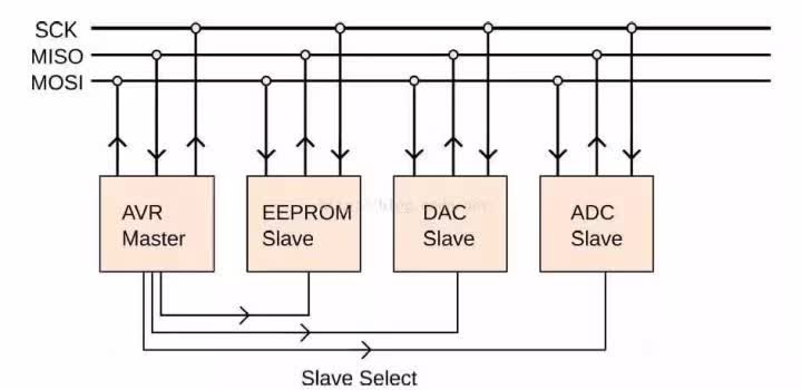
The data transfer between SPI devices is also called data exchange because the SPI protocol stipulates that an SPI device cannot only act as a "Transmitter" or "Receiver" during data communication. During each Clock cycle, the SPI device will send and receive a bit-sized data, which is equivalent to the device having a bit size of data exchanged. A slave device must receive the control signal sent by the Master. It can be accessed by the Master device before. Therefore, the Master device must first select the slave device through the SS/CS pin and select the slave device you want to access. During the data transmission, each time it receives The data must be sampled before the next data transmission. If the previously received data is not read, then the data that has been received will be discarded, resulting in the SPI physical module eventually failing. Therefore, it is generally in the program. After the SPI transfers the data, read the data in the SPI device, even if the data (Dummy Data) is not in our program. use.
2.4 SPI has four transmission modesThe rising edge, falling edge, leading edge, and trailing edge trigger. Of course, there are also MSB and LSB transmission methods.
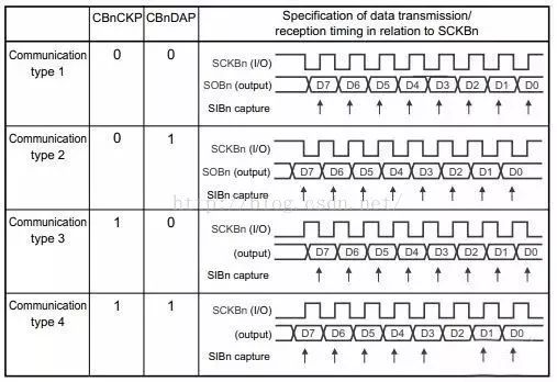
There is no read or write statement because essentially every time the SPI is a master-slave device exchanging data. In other words, if you send a data, you will inevitably receive a data; if you want to receive a data, you must also send a data first.
3. Working mechanism 3.1 Overview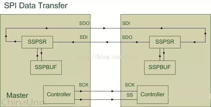
The above figure is just a brief description of the communication between SPI devices. Here are some of the modules shown in the figure: SSPBUF, Synchronous Serial Port Buffer, which refers to the internal buffer inside the SPI device. Physically, it is a FIFO format that stores temporary data during transmission; SSPSR, Synchronous Serial Port Register, refers to the shift register (Shift Regitser) in the SPI device, which functions according to the set data bit width (bit). -width) Move data into or out of SSPBUF; Controller, which refers to the control registers in the SPI device, can be configured to set the transfer mode of the SPI bus. Normally, we only need to program the four pins described in the above figure to control the data communication between the entire SPI device: SCK, Serial Clock, the main function is to transfer the clock from the master device to the slave device. Signal, control timing and rate of data exchange; SS/CS, Slave Select/Chip Select, for Master device chip select Slave device, enable selected Slave device to be accessed by Master device; SDO/MOSI, Serial Data Output/ Master Out Slave In, also known as Tx-Channel on the Master, is used as the data exit, mainly used for sending data by SPI device; SDI/MISO, Serial Data Input/Master In Slave Out, also known as Rx on Master. -Channel, as the data entry, is mainly used for receiving data by the SPI device; during the communication process, the SPI device generates a data link loop between the Master device and the slave device, as shown in the figure above. That way, through the SDO and SDI pins, the SSPSR control data is shifted in and out of the SSPBUF, the Controller determines the communication mode of the SPI bus, and the SCK transmits the clock signal.
3.2 Timing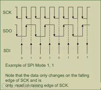
The above figure illustrates the working mechanism of the SPI protocol by exchanging 1 Byte data between the Master device and the Slave device. First, explain the concept of phase and polarity here.
3.2.1 SPI related abbreviations or statementsSPI Polarity and Phase Phase, the most common notation is CPOL and CPHA, but there are some other ways to write it up as follows: (1) CKPOL (Clock Polarity) = CPOL = POL = Polarity = (clock) polarity (2 CKPHA (Clock Phase) = CPHA = PHA = Phase = (clock) phase (3) SCK = SCLK = SPI clock (4) Edge = edge, that is, the moment when the clock level changes, ie rising edge or The falling edge has two edges for one clock cycle, called: Leading edge=previous edge=first edge. For the starting voltage is 1, then when 1 becomes 0, start The voltage is 0, then 0 is changed to 1; Trailing edge = the next edge = the second edge, for the starting voltage is 1, then 0 becomes 1 (that is, after the first 1 becomes 0) , it is possible that the following 0 becomes 1), for the starting voltage is 0, then when 1 becomes 0;
3.2.2 Phase and Polarity of SPICPOL and CPHA, respectively, can be 0 or hour 1, and the corresponding four combinations are: Mode 0 CPOL=0, CPHA=0Mode 1 CPOL=0, CPHA=1Mode 2 CPOL=1, CPHA=0Mode 3 CPOL=1, CPHA=1
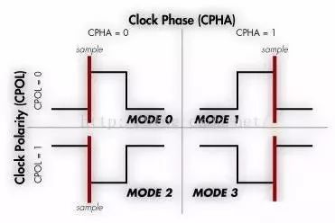
First, what is the idle time of the SCLK clock, which is the state before and after the SCLK is sent 8 bits of data, corresponding to this, when the SCLK is transmitting data, it is normal working, effective active It’s time. Let me speak English first, and its simplification is explained as: Clock Polarity = IDLE state of SCK. Then use Chinese detailed explanation: SPI CPOL, when the SCLK idle idle, its level value is low level 0 or high level 1: CPOL=0, the level of the clock idle idle is low level, so When SCLK is valid, it is high level, which is called active-high; CPOL=1, the level of the clock idle idle is high level, so when SCLK is valid, it is low level, so-called active -low;
3.2.4 CPHA phaseFirst of all, capture strobe = latch = read = sample, which means that the data is sampled and the data is valid. The phase corresponds to whether the data sample is at the first edge, whether it is the first edge or the second edge, 0 corresponds to the first edge, and 1 corresponds to the second edge. For: CPHA=0, indicating the first edge: For CPOL=0, the idle time is low, the first edge is from low to high, so it is the rising edge; for CPOL=1, the idle time is High level, the first edge is from high to low, so it is the falling edge; CPHA=1, indicating the second edge: for CPOL=0, idle is low, the second edge is high Change to low, so it is a falling edge; for CPOL=1, idle is high, the first edge is from low to high, so it is a rising edge; or the above figure is easier to understand
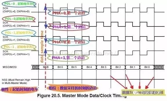
The SPI is divided into a master device and a slave device, and the two communicate through the SPI protocol. The mode of setting the SPI is the mode of the slave device, which determines the mode of the master device. So first understand the mode of the SPI from the device, and then set the mode of the SPI of the master device to the same mode as the slave device to communicate normally. There are two modes for the slave SPI:
3.2.5.1 fixed, with SPI determined from device hardwareSPI slave device, specifically what mode, related datasheet will be described, you need to find the relevant description in the datasheet, that is: on the SPI slave device, when idle, is high or low, that is, Whether CPOL is 0 or 1; then find out whether the device is sampling data on the rising edge or the falling edge. Thus, under the premise that the value of CPOL is determined, it can be estimated that CPHA is 0 or 1.
3.2.5.2 Configurable, set by the software itselfThe slave device is also an SPI controller, which is supported in all four modes. In this case, you only need to set it to a certain mode. Then, after knowing the mode of the slave device, set the mode of the SPI master device to be the same as the slave device mode. For how to configure SPI CPOL and CPHA, not to mention in detail, most of them are directly to write the corresponding two bits of CPOL and CPHA in the corresponding register of the corresponding SPI controller, write 0 or write 1. 3.3 SSPSR
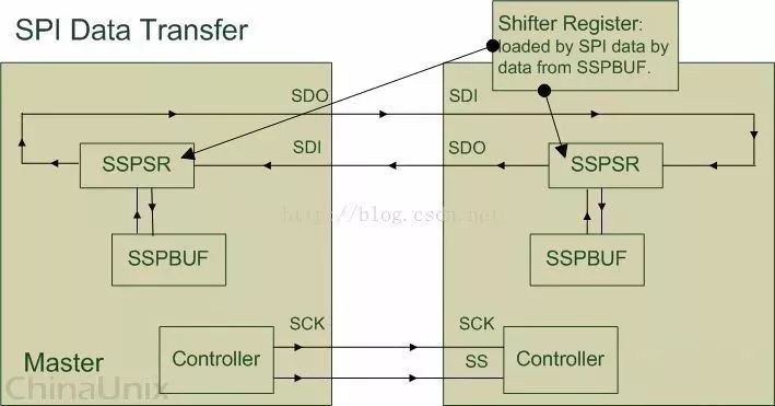
The SSPSR is the internal shift register (Shift Register) of the SPI device. Its main function is to move in or out of the data in the SSPBUF according to the state of the SPI clock signal. The data size of each move is determined by Bus-Width and Channel-Width. The role of Bus-Width is to specify the unit of data transfer between the address bus and the master device. For example, we want to write 16 Bytes of data to the SSPBUF in the Master device: First, set the Bus-Width to the configuration register of the Master device. Byte; then write data to the Tx-Data shift register of the master device at the address of the address bus, write 1 Byte of data each time (using the writeb function); after writing 1 Byte of data, the Tx inside the Master device The -Data shift register automatically transfers 1 Byte of data from the address bus into the SSPBUF; the above actions need to be repeated 16 times. The purpose of Channel-Width is to specify the unit of data transfer between the Master and the Slave device. Similar to Bus-Width, the shift register inside the Master device automatically transfers data from the Master-SSPBUF through the Master-SDO pin to the Slave-SDI pin in the Slave device according to Channel-Width. Slave-SSPSR then The received data is moved into the Slave-SSPBUF. Normally, the Bus-Width will always be greater than or equal to the Channel-Width, which will ensure that the Master will not appear. The frequency of data exchange with Slave is faster than the data exchange frequency between the address bus and the Master, resulting in the situation where the data stored in the SSPBUF is invalid data.
3.4 SSPBUF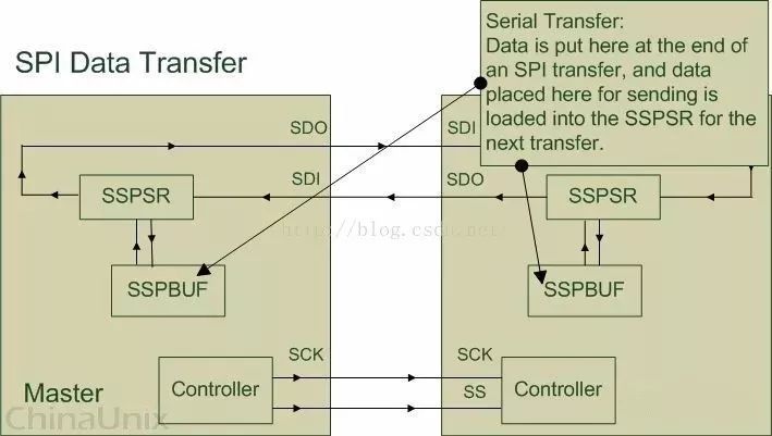
We know that the data exchanged between the Master and the Slave in each clock cycle is actually the SPI internal shift register copied from the SSPBUF. We can pass the register corresponding to the SSPBUF (Tx-Data / Rx-Data register) Read and write data, and control the SSPBUF inside the SPI device. For example, before sending data, we should first write the data to be sent to the Master's Tx-Data register, which will be based on the Master-SSPSR shift register. Bus-Width is automatically moved into the Master-SSPBUF, and then the data is removed from the Master-SSPBUF by the Master-SSPSR according to the Channel-Width, passed to the Slave-SDI pin through the Master-SDO pin, and the Slave-SSPSR is taken from the Slave-SSPSR. The data received by Slave-SDI is moved into Slave-SSPBUF. At the same time, the data in Slave-SSPBUF is sent to Master-SDI via Slave-SDO according to the size of each received data (Channel-Width). Master-SSPSR The data received from the Master-SDI is transferred to the Master-SSPBUF. After a single data transfer is completed, the user program can read the Master device data from the Rx-Data register of the Master device. Exchange the resulting data.
3.5 Controller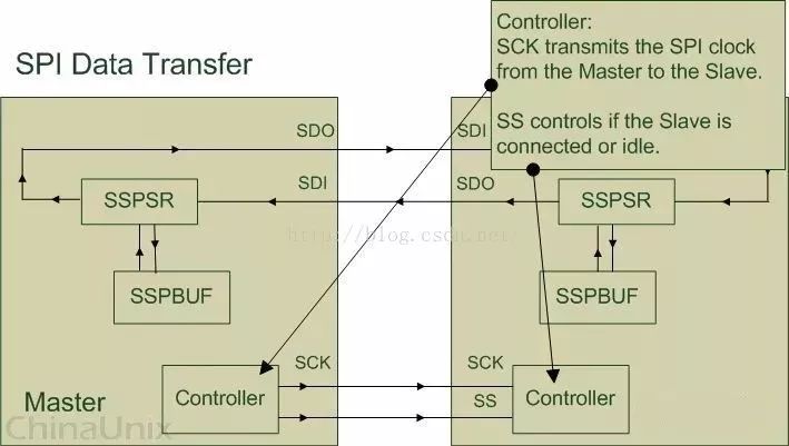
The Controller in the Master device mainly controls the slave device through the Clock Signal and the Slave Select Signal. The Slave device waits until it receives the chip select signal sent by the Master device, and then according to the clock signal. The chip select operation of the working master device must be implemented by the program. For example: The program pulls the clock signal of the SS/CS pin low to complete the preliminary work of the SPI device data communication; when the program wants the SPI device to end the data communication Then, the clock signal on the SS/CS pin is pulled high.
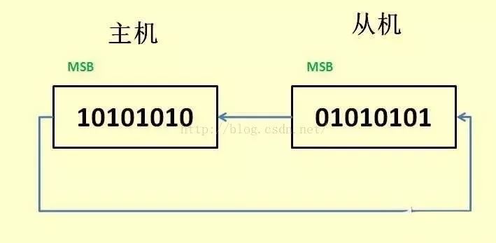
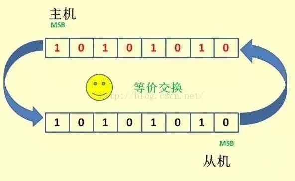
4. SPI exampleI have said so much above, here I will give an example to help you understand. SPI is a ring bus structure, composed of ss (cs), sck, sdi, sdo, the timing is actually very simple, mainly under the control of sck, two bidirectional shift registers for data exchange. Assume that the following 8-bit register is loaded with data 10101010 to be transmitted, rising edge transmission, falling edge reception, and high-order transmission. Then the data will be sdo=1 when the first rising edge comes; register=0101010x. When the falling edge comes, the level on sdi will be stored in the register, then the register = 0101010sdi, so after 8 clock pulses, the contents of the two registers are exchanged once. This completes a spi timing. Example: Assume that the master and slave are ready to initialize: and the sbuff=0xaa of the master and the sbuff=0x55 of the slave. The following will demonstrate the data of the 8 clock cycles of the spi step by step: assuming the rising edge sends data.
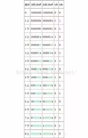
This completes the 8-bit exchange of two registers. The upper one indicates the rising edge and the lower indicates the falling edge, and sdi and sdo are relative to the host. Already very close to understanding, the next step is to turn the above process into an animation
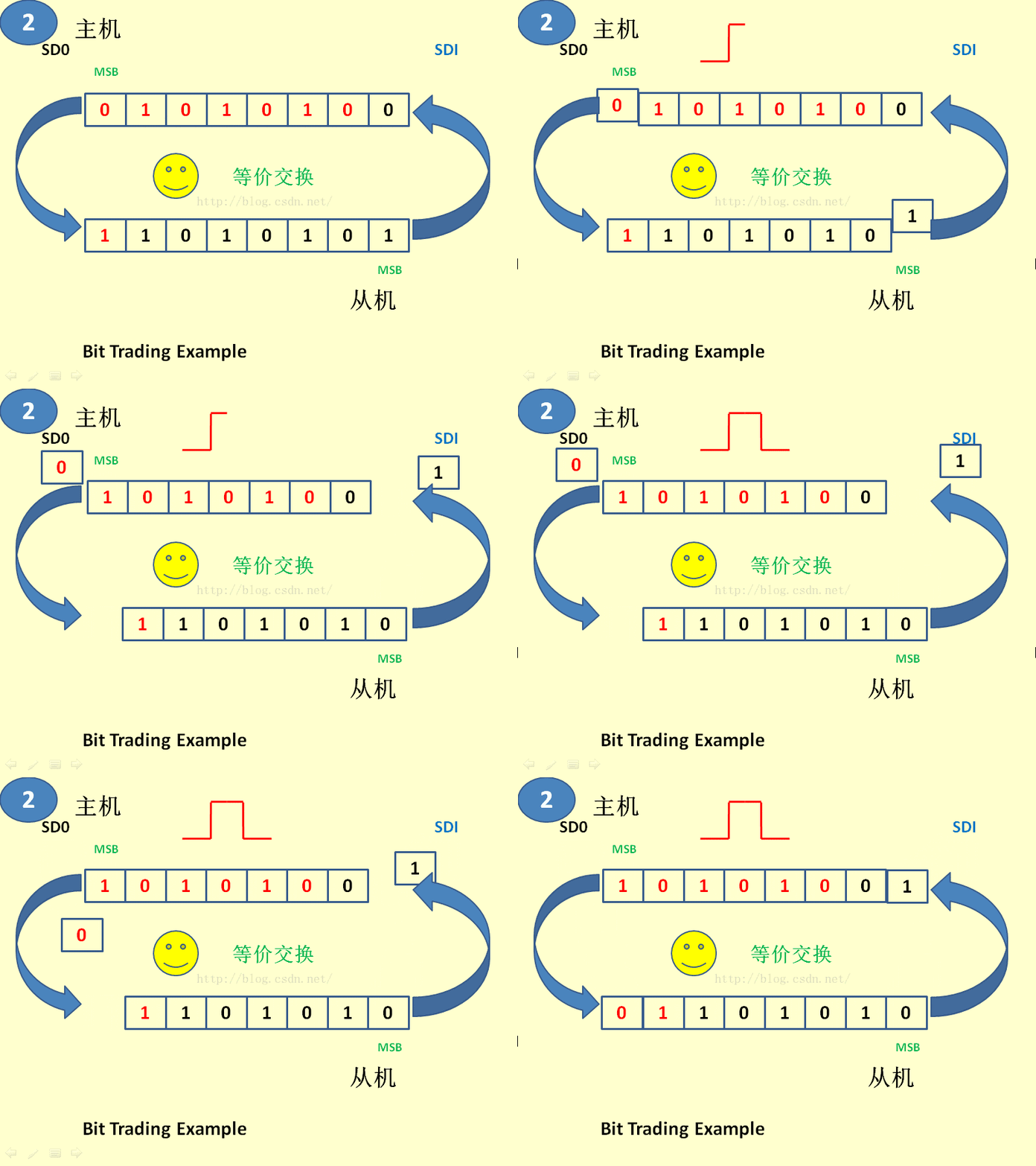
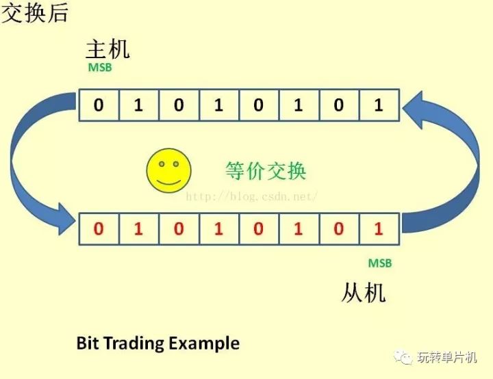
STM32's spi is simpler because STM32 integrates SPI internally.
5.1 SPI initialization[cpp] view plaincopy
Void SPIInit(void)
{
SPI_InitTypeDef SPI_InitStructure;
/ / Initialize the connection between SPI and GPIO port
FLASH_GPIO_Init();
/*!< Deselect the FLASH: Chip Select high */
CE_High();
/*!< SPI configuration */
SPI_InitStructure.SPI_Direction = SPI_Direction_2Lines_FullDuplex;
SPI_InitStructure.SPI_Mode = SPI_Mode_Master;
SPI_InitStructure.SPI_DataSize = SPI_DataSize_8b;
SPI_InitStructure.SPI_CPOL = SPI_CPOL_High;
SPI_InitStructure.SPI_CPHA = SPI_CPHA_2Edge;
SPI_InitStructure.SPI_NSS = SPI_NSS_Soft;
SPI_InitStructure.SPI_BaudRatePrescaler = SPI_BaudRatePrescaler_8;
SPI_InitStructure.SPI_FirstBit = SPI_FirstBit_MSB;
SPI_InitStructure.SPI_CRCPolynomial = 7;
SPI_Init(SPI1, &SPI_InitStructure);
/*!< Enable the sFLASH_SPI */
SPI_Cmd (SPI1, ENABLE);
}
5.2 SPI write 1 byte[cpp] view plaincopy
Uint8 Send_Byte(uint8 data)
{
//Send is not empty
While(!(SPI1->SR & SPI_I2S_FLAG_TXE));
SPI1->DR = data;
/ / Read the received data
While(!(SPI1->SR & SPI_I2S_FLAG_RXNE));
Return SPI1->DR;
}
5.3 SPI reads a byte[cpp] view plaincopy
Uint8 Get_Byte(void)
{
//Send is not empty
While(!(SPI1->SR & SPI_I2S_FLAG_TXE)); // The send buffer is empty, jumping out of the loop
SPI1->DR = 0xFF; //
/ / Read the received data
While(!(SPI1->SR & SPI_I2S_FLAG_RXNE)); //Accept buffer is not empty, jump out of the loop
Return SPI1->DR;
}
The utility model provides a disposable electronic cigarette, comprising: a hollow shell, the bottom of the shell is provided with a lower cover; the shell contains an atomizer, and the outer side of the atomizer is sheathed with a disposable cigarette A bomb, a microphone cover is arranged under the atomizer, a microphone is covered under the microphone cover, a battery is arranged on one side of the atomizer, and an upper cover is arranged on the top of the casing; The atomizer includes an atomizing core, an oil-absorbing cotton sleeved on the outside of the atomizing core, and an atomizer outer tube sleeved on the outside of the oil-absorbing cotton. The disposable electronic cigarette provided by the utility model absorbs the smoke oil on the surface through the absorbing cotton, and then atomizes the smoke through the atomizing core, which greatly reduces the risk of oil leakage, at the same time, reduces the burning of cotton and ensures the smoking taste.The utility model provides a disposable electronic cigarette, comprising: a hollow shell, the bottom of the shell is provided with a lower cover; the shell contains an atomizer, and the outer side of the atomizer is sheathed with a disposable cigarette A bomb, a microphone cover is arranged under the atomizer, a microphone is covered under the microphone cover, a battery is arranged on one side of the atomizer, and an upper cover is arranged on the top of the casing; The atomizer includes an atomizing core, an oil-absorbing cotton sleeved on the outside of the atomizing core, and an atomizer outer tube sleeved on the outside of the oil-absorbing cotton. The disposable electronic cigarette provided by the utility model absorbs the smoke oil on the surface through the absorbing cotton, and then atomizes the smoke through the atomizing core, which greatly reduces the risk of oil leakage, at the same time, reduces the burning of cotton and ensures the smoking taste.The utility model provides a disposable electronic cigarette, comprising: a hollow shell, the bottom of the shell is provided with a lower cover; the shell contains an atomizer, and the outer side of the atomizer is sheathed with a disposable cigarette A bomb, a microphone cover is arranged under the atomizer, a microphone is covered under the microphone cover, a battery is arranged on one side of the atomizer, and an upper cover is arranged on the top of the casing; The atomizer includes an atomizing core, an oil-absorbing cotton sleeved on the outside of the atomizing core, and an atomizer outer tube sleeved on the outside of the oil-absorbing cotton. The disposable electronic cigarette provided by the utility model absorbs the smoke oil on the surface through the absorbing cotton, and then atomizes the smoke through the atomizing core, which greatly reduces the risk of oil leakage, at the same time, reduces the burning of cotton and ensures the smoking taste.
maskking vape,maskking vape price,maskking vape review,maskking vape shop,,maskking vape cost,maskking vape disposable,maskking vape informacion
Suizhou simi intelligent technology development co., LTD , https://www.msmsmart.com