CPLD design of I2C device interface IP core
According to the characteristics of the serial expansion of the I2C of the single-chip microcomputer, the IP core is established by using the AHDL language in the environment of the EDA software MaxplusII. This design is implemented by a state machine. The design process is described at the same time as the IP core is established and downloaded to the chip for verification by hardware test.
Keywords: programmable logic device I2C serial extended IP core
Due to the trend of CPLD digital design structuring, there will be IP (Intellectual Property) cores for different levels of CPLD. Individual IP cores can be reused, greatly improving design capabilities and efficiency. Major foreign companies have launched special IP cores, and China urgently needs to develop its own IP core. In this paper, the design process and results are given in detail for the characteristics of I2C's main mode serial extended communication.
1 IP core introduction
IP core refers to: some functional blocks that are commonly used in digital circuits but are more complicated, such as FIR filters, SDRAM controllers, PCI interfaces, etc., are designed as modules with modifiable parameters, so that other users can directly call these modules to Avoid duplication of work. As the size of CPLD/FPGA grows larger and the design becomes more complex, the use of IP cores is a trend. Many companies recommend using off-the-shelf or tested megafunctions and IP cores to enhance existing HDL design methods. When performing complex system design, these megafunctions and IP cores will undoubtedly greatly reduce design risks and shorten development cycles. Using these megafunctions and IP cores will put more time and effort into improving and improving system-level products without having to re-open the discovered megafunctions and IP cores. The construction of China's IP nuclear pool has become quite urgent, and it is an important goal of the development of the integrated circuit industry.
2 Introduction to I2C serial communication features
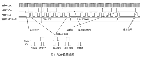
The I2C software and hardware protocol introduced by Philips is very clever. In the single-master I2C bus system, there is only one single-chip microcomputer on the bus, and the rest are peripheral devices with I2C bus. Since only one single-chip microcomputer becomes the master node on the bus, the single-chip system always occupies the bus, and there is no competition. The master node does not have to have its own node address. As long as each peripheral device has its own device address, two I/O lines SCL (clock line) and SDA (data line) can virtualize the I2C bus interface. The data transfer on the I2C bus is shown in Figure 1. Each frame of data transmitted on the bus is 1 byte. After the bus is started, it is required that each time a byte is transmitted, the other party responds with an acknowledge bit. When sending, the highest bit is sent first. There is a start signal at the beginning of each transfer and a stop signal at the end. After the bus has transferred 1 byte, the transmission can be suspended by controlling the clock line. At this time, SCL can be made low after the response signal, and the control bus is suspended. The same method can be used when the master node requests a bus pause. Figure 1 shows the CPLD sending two data, 01010011 and 01001001, to a peripheral I2C device.
3 Establishment of I2C serial extended IP core in MaxplusII environment
MaxplusII is EDA software for CPLD in Altera, USA. There are many commonly used macro cells, such as counters, four arithmetic, various logic gates, and even ROM and RAM. The specific parameters in these macrocells can be set by the user, which is the IP core form mentioned above. It avoids duplication of effort and improves efficiency. The following will design the IP core of the lower computer.
Maxplus II's AHDL (Altera Hard ware DescripTIon Language) is a modular high-level language developed by Altera Corporation that is fully integrated into Maxplus II. It is especially suitable for describing complex combinatorial logic, group operations, state machines and truth tables. This article uses AHDL to directly generate IP cores.
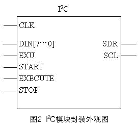
The ultimate goal of the design is to generate the Symbol as shown in Figure 2. The purpose of controlling SDA and SCL is achieved by inputting data, and the signal is transmitted to the I2C device at the required timing.
The design idea is to use the state machine to achieve timing. It mainly includes state machines such as input data latching, start, data transmission, and stop. Through the state machine, it is determined in each state that the next state SDA and SCL are high or low, in this way, each timing required by I2C is realized. Because of the use of AHDL, this state machine is very convenient to implement, and the program is simple and clear. Due to space limitations, only the state machine for data transfer is introduced. The state diagram is shown in Figure 3.
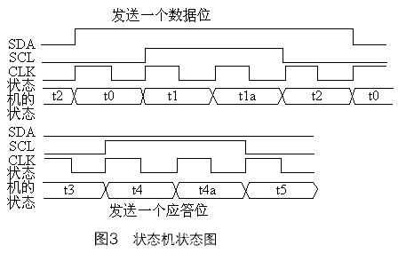
In the following program, Cmd_reg2 is the transmit enable scratch bit; Sh_reg[] is the data latch, and by the left shift, the highest bit data Sh_reg7 is currently transmitting data and stored in SDA_tmp. Through the comparison procedure of Figure 3, it can be seen that a detailed process of transmitting data bits using state machines can be seen. The list of procedures is as follows:
IF Cmd_reg2 THEN -- If "send enable", use Sh_reg7 as the current transmit bit SDA_tmp = Sh_reg7; ELSE SDA_tmp = VCC; END IF; St.clk = SysClk; St.ena = BaudGen; CASE St IS - Control Transfer 8 State machine for bit data WHEN t0 => IF Cmd_reg2 OR Cmd_reg3 THEN SDA = SDA_tmp; -- Start transmitting data SCL = GND; St = t1; ELSE St = t0; END IF; WHEN t1 => SCL = VCC; SDA = SDA_tmp ; St = t1a; WHEN t1a => SCL = VCC; SDA = SDA_tmp; St = t2; WHEN t2 => Sh_reg[7..1] = Sh_reg[6..0]; -- The data is shifted to the left, taking the high position Sh_reg [0] = GND; Sh_reg[].ena = EXU; SCL = GND; SDA = SDA_tmp; IF Bit[] == 7 THEN -- If the 8 bits are transmitted, the acknowledge bit is sent; otherwise, St = t3; ELSE St = t0; END IF; WHEN t3 => -- Send acknowledge bit SDA = GND; St = t4; WHEN t4 => SDA = GND; SCL = VCC; St = t4a; WHEN t4a => SDA = GND; SCL = VCC; St = t5; WHEN t5 => SCL = GND; St = t6; WHEN t6 => SDA = GND; FINISHED = VCC; St = t0; END CASE; Bit[] = Bit[] + 1; - Transfer one bit, the number of transmitted bits plus one
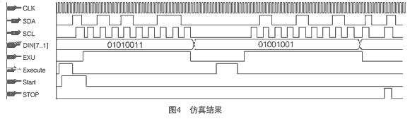
Figure 4 shows the simulation results. After the start signal is given, two 8-bit data are transmitted: each data is followed by an acknowledge bit, and after the first data request is delivered, the pause is for a period of time, and then the second data is transmitted; Later, the host sends a stop delivery request, which gives a stop signal. These signals are fully compliant with I2C timing requirements on SDA and SCL. To achieve a bus transfer rate that is improved by 400 kb/s, since the above description requires 4 clock cycles per 1-bit data, the given clock is 1600 kHz. In Figure 4, Execute is the execution signal, that is, when it is high, the input data DIN[7..0] is valid; EXU is the transmit enable signal, and only when it is high, can serial data be sent to the peripheral device. ; Start is the start control signal for the start signal; STOP is used to inform the end of the bus data transmission, a stop signal occurs.
After the simulation, the generated pof file is downloaded to the FPGA board EPM7128SLC84-6 by the ISP (in system programming) by the programming cable. The I/O ports SDA and SCL are connected with pull-up resistors, and two I2C devices are connected to the SAA1064 (LED display I2C string). Tested in and out of the chip, the CPLD uses the IP core of the I2C, works normally, and can be displayed as required.
References 1 Altera. ALTERA DIGITAL LIBRARY 2000 2 He Limin. Advanced Microcontroller. Beijing: Beijing University of Aeronautics and Astronautics Press, 2000 3 Zhao Zhaoguang. Principles, Development and Application of Programmable Logic Devices. Xidian University Press, 2000 4 SAA1064 Product SpecificaTIon Philps.
Antenk DIN41612 Connectors are a versatile two piece PCB connector set with feaures useful for many applications including connections for plug-in card and back-panel wiring, PCB to PCB attachment and peripheral connections for external interfaces. Features include a multitude of body sizes and styles with options that include selective contact loading, make and break contacts, contact lead length choices and contact plating variations each in .100" [2.54mm] or .200" [5.08mm] centerline spacing.
The DIN 41612 standard covers a series of two-piece backplane connectors widely used in rack-based telecommunication, computing, process control, medical, industrial automation, test and measurement and military/aerospace systems where long-term reliability is required. They consist of one to three rows of contacts in combinations of 16, 32, 48, 64, or 96 contacts on a 0.1-inch (2.54 mm) grid pitch. The 3 rows are labelled a, b and c and connectors up to 64 way if using a 96 way body can use either rows a+b or a+c. DIN 41612 Signal connectors can be rated to 1.5 amps per signal pin, at 500 volts, although these figures may be de-rated according to safety requirements or environmental conditions. Several hybrid power and coaxial configurations are available that can handle up to 5.6A or even 15A. This wealth of variations explains the very wide range of applications that they`re put to. For over 30 years these DIN 41612 `Euro Card` connectors to IEC 60603-2 have offered a highly reliable system for board interconnects. Precision contact density, low mating forces, a two piece protective design and many contact termination styles offer unlimited design opportunities. Termination methods include – straight PC, solder eyelet, wire wrap, crimp and [press fit" terminals. Insertion and removal force are controlled, and three durability grades are available. Standardisation of the connectors is a prerequisite for open systems, where users expect components from different suppliers to operate together; ept and Conec DIN 41612 are therefore fully intermateable with all other similarly compliant products from other manufacturers like Harting, Erni, Hirose and TE Connectivity, etc.
The most common connector in the DIN product line is type C, which is widely used in VMEbus systems, the DIN 41612 standard has been upgraded to meet international standards IEC 60603-2 and EN 60603-2. In the past, ept used a comb supported press-fit tool for their type C and B press-fit female connectors. To be more competitive, ept has changed to flat-rock technology (just a flat piece of steel pushed on the top of the connector) as used by many other manufacturers.
DIN 41612 Connectors are widely used in rack-based electrical systems. The standard performance of these connectors is a 2 A per pin current carrying capacity and 500 V working voltage. Both figures may be variable due to safety and environmental conditions.
Types
Number of contacts varies
Many variations of housing material, including different types of metal and plastic
Both angled and straight versions
Male and female
C,R,B,Q Type DIN41612 Connectors

Half C, R, B & Q Type DIN41612 Connectors

1/3 C,R, B & Q Type DIN41612 Connectors

H, F, H+F & M type DIN41612 Connectors

IDC Type DIN41612 Connectors

Female Cable Connector

High Pin Count DIN41612 Connectors

Shroud DIN41612 Connectors

Features and Benefits of Din41612 Connector:
• Indirect mating (male/female)
• Automated production processes
• Continuous quality assurance
• 3-160 contacts
• Complete interconnection system
• Numerous interface connectors
• A wide variety of hoods
• Many termination technologies provide for the lowest installed cost
• Contacts selectively gold-plated
• Tinned terminations for increased solderability
Uses
The primary use of DIN 41612 connectors are PCB Connectors and motherboards, the main acceptance would be their board to board reliable connections.
Applications of Din41612 Connector:
Applications
• Data centers
• Storage
• Servers
• Base stations
• Telecommunications equipment
• Backplane and motherboard assemblies
• Switching systems
• Modular rack systems
• Power automation
• Distributed control systems in
industrial control
• Programmable logic controllers (PLC)
• Robotics
• Test and lab equipment
• Energy distribution
• Monitoring equipment
This is not a definitive list of applications for this product. It represents some of the more common uses.
Din41612 Connector,Din 41612,Eurocard Connector Din41612,Male Din41612 Connector
ShenZhen Antenk Electronics Co,Ltd , https://www.antenksocket.com