Researchers at the University of California, Berkeley, showcased three-five (III-V) family of nanopillar LED designs that are compatible with Si-CMOS optical lithography , while also controlling the precise growth of these nano-LEDs. It is a key element for efficient integration of photons in CMOS circuits for fast on-chip optical interconnects.
In the "ACS Photonics" journal, the researchers published "InP nanopillar LEDs on silicon with bright electroluminescence on silicon crystals with teleluminescent wavelengths" (Ultracompact Position-Controlled InP Nanopillar LEDs on Silicon with Bright Electroluminescence at Telecommunication) Wavelengths) pointed out that the growth rate of the growth position is as high as 90%, and a uniform array of indium phosphide (InP) nanopillars can be realized on the silicon crystal, and grown under CMOS compatible conditions: low temperature and no catalyst.

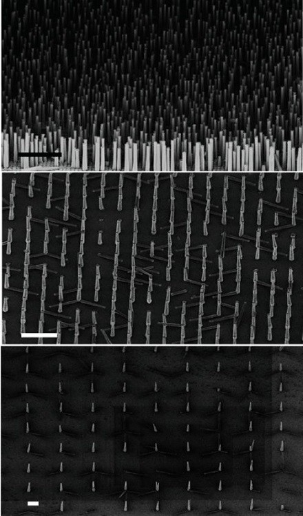
A low-magnification SEM image of a position-controllable InP nanopillar array grown at 460 °C. The scales in all images correspond to 10 μm and 1 μm, 4 μm and 40 μm growth cycles (pitch).
The researchers began with a clean silicon wafer (111), depositing 140 nm of dioxide into a nanometer-scale pore diameter of about 320 nm at 350 ° C, and positioning the nanocolumn nucleation sites at a pitch of 1 μm - 40 μm. After the researchers chemically roughened the surface of the silicon crystal, the InP nanostructures were grown in the MOCVD chamber at a temperature of 450 ° C to 460 ° C. The researchers found that the cone angle of the nanocolumn is significantly affected by the growth temperature, producing nanoneedles at 450 °C and almost vertical columnar structures at 460 °C.
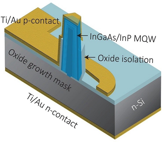
Based on these nanopillars, the researchers incorporated five indium gallium arsenide (InGaAs) quantum wells into the active region of the pn diode through a concentric core-shell growth to form an electrically driven n-InP/InGaAs MQW/p-InP/p-InGaAs nano-LED.

Nano column MQW LED assembly schematic
Due to the core-shell growth pattern, the nanopillars grow from their nucleation sites and extend beyond the oxide openings to a final diameter of about 1 μm. Thus, when the n-doped core of the nano-pillar is in direct contact with the n-Si substrate, the p-doped outer shell grows on the oxide shield, eliminating the shunt path from the p-doped outer shell and the n-Si substrate. 20/200 nm Ti/Au is evaporated by a tilted electron beam to a highly p-doped InGaAs contact layer, completing the assembly to form an electrical contact, wherein a small portion of the nano-pillar is exposed and no metal is emitted as LED light. window.
Characterization of nano-columnar LEDs was performed at 1510 nm and a quantum efficiency of about 30%. Although the nanopillar LED has a small footprint, it can output 4μW, which researchers claim is the highest light output record that can be achieved from nanopillar/nanostructured LEDs. Under this build, the available light output is reduced to 200nW due to a collection efficiency of only 5%.
Another interesting aspect of the study is that the component can generate optical gain with electrical bias and exhibit a strong photoresistance during reverse injection, which helps to achieve photonic integration on the chip.
For more LED related information, please click on the LED network or follow the WeChat public account (cnledw2013).
China Ev Charging Pile,Advertising Charging Station supplier & manufacturer, offer low price, high quality Advertising Charging Pile,Advertising Charging Pile, etc.
Ev Charging Pile,Advertising Charging Station,Advertising Charging Pile,Advertising Charging Pile
Shenzhen Hongjiali New Energy Co., Ltd. , https://www.hjlcharger.com