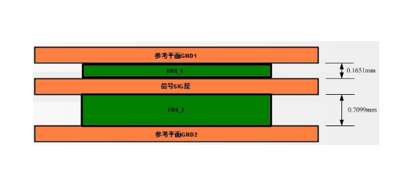
First, the power plane and ground plane must meet the 20H rule
Second, when the power layer, the number of the bottom layer and the number of trace layers of the signal are determined, in order to make the PCB have good EMC performance, the basic requirements for the relative arrangement position between them are as follows:
Below the component layer (the second layer) is the ground plane, providing a device shield and providing a reference plane for the top layer wiring.
All signal layers are as close as possible to the ground plane
Try to avoid the two signal layer traces adjacent. If it is unavoidable, the spacing of the adjacent signal layers should be increased. The two signal lines are vertically aligned at the upper and lower positions.
The main power source should be adjacent to it as far as possible, and the distance between the power source and the ground plane should be reduced as much as possible, preferably less than 5 mils, preferably not more than 10 mils.
The symmetrical stacking of the laminated structure also takes into account the PCB manufacturing process and the warpage of the control PCB. Generally, civilian products adopt the IPC_II standard, which requires the PCB warpage to be less than 0.75%.
Use even layer structure.

Third, the common PCB laminate structure
1. The laminated structure of the four-layer board:
TOP, GND02, PWR03, BOTTOM; (The complete ground plane below the TOP layer is the optimal wiring layer, the key signal should be placed preferentially in this layer. The distance between the power plane and the ground plane should not be too thick, preferably no more than 5mil)
TOP, PWR02, GND03, BOTTOM; (this scheme is similar to scheme a)
GND01, S02, S03, GND04/PWR04 (this scheme is sometimes used to achieve a certain shielding effect)
2, the laminated structure of the six-layer board
TOP, GND02, S03, PWR04, GND05, BOTTOM (This solution is the industry's main push layer design of 6-layer PCB, with 3 wiring layers, one power plane, 2 ground planes. Between layers 4 and 5 The thickness should be as small as possible. The 3 layers are the best wiring layer, telling the signal and the high-risk signal is preferentially placed on this layer)
TOP, GND02, S03, S04, PWR05, BOTTOM (This can be used when the number of wiring layers required is large and the cost is critical. In this scheme, S03 is the optimal wiring layer)
TOP, S02, GND03, PWR04, S05, BOTTOM (the thickness of the core between the 3rd and 4th layers is as small as possible so that the power supply impedance is low, the first and second layers are to be cross-routed, and the 5th and 6th layers are to be cross-routed. S02 near the ground plane is the optimal wiring layer)
3. Laminated structure of eight-layer board
TOP, GND02, S03, GND04, PWR05, S06, GND07, BOTTOM (the industry's main push stacking scheme, S03 is the optimal wiring layer)
TOP, GND02, S03, PWR1_04, GND05, S06, PWR2_07, BOTTOM (This scheme is used for a variety of power supplies, using a power plane that cannot meet the PCB power supply requirements, PCB power supply crossover; Layer 3 and Layer 6 Is the best wiring layer)
TOP, GND1_02, S03, S04, PWR05, GND2_07, BOTTOM (The decoupling effect of this laminated structure power plane and ground plane is very poor, generally used in designs with more wiring layers and strict cost control, such as consumer The second layer and the sixth layer are better wiring layers. Generally, in the flat panel design, DDR and other high speed signals are classified according to signal properties and then arranged in the TOP layer, the third layer, the sixth layer, and the eighth layer. The stack design should increase the distance between the 3rd and 4th layers and cross the line)
4. Laminated structure of ten layers
TOP, GND1_02, S03, S04, GND2_05, PWR06, S07, S08, GND3_09, BOTTOM (single power plane scheme is preferred to use this stacking scheme)
TOP, GND1_02, S03, S04, PWR1_05, GND2_06, S07, S08, PWR2_09, BOTTOM (3, 7 layers are the best wiring layer)
TOP, GND1_02, S03, GND2_04, PWR1_05, PWR2_06, GND3_07, S08, GND4_09, BOTTOM (This scheme is recommended when the cost is not high, EMC requirements are high, and dual power plane power supply requirements are required; 3 and 8 layers are the most Excellent wiring layer, you can increase the distance between the two power planes of 5 and 6 layers)
Keystone Jack,cat6 keystone,cat6 jack,cat6 wall jack
NINGBO UONICORE ELECTRONICS CO., LTD , https://www.uniconmelectronics.com