Today's high-speed digital systems can have clock frequencies as high as hundreds of megahertz, and their fast-slope transients and extremely high operating frequencies, as well as the large circuit density, will surely make the system appear to behave differently from low-speed designs. Signal integrity issues. Destroying signal integrity directly leads to signal distortion, timing errors, and incorrect data, address, and control signals, causing system misoperations and even system crashes. Therefore, signal integrity issues have increasingly attracted the attention of high-speed digital circuit designers.
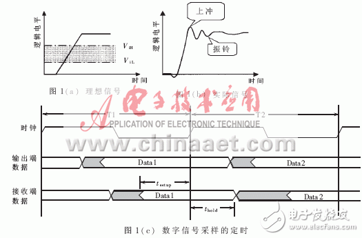
1 Signal integrity problem and its mechanismSignal Integrity (SI) relates to the accuracy of signal quality and signal timing on the transmission line. In the digital system, for logic 1 and 0, there is always a corresponding reference voltage, as shown in Figure 1 (a): the level higher than ViH is logic 1, and the level lower than ViL is regarded as logic 0, The shaded area can be considered as an indeterminate state. As can be seen from Figure 1(b), the actual signal always has an overshoot, an undershoot, and a ringing, and its oscillation level is likely to fall into the uncertainty region of the shadow portion. The transmission delay of the signal directly leads to inaccurate timing. If the timing is not appropriate enough, it is very likely to get inaccurate logic. For example, if the signal transmission delay is too large, it is very likely that no accurate logic will be obtained at the rising or falling edge of the clock. The general digital chip requires that the data must be stable before the tsetup of the clock trigger edge to ensure the timing of the logic is accurate (see Figure 1 (c)). For an actual high-speed digital system, the signal may be worse than we think due to electromagnetic interference and other factors, so the requirements for tsetup are more demanding. At this time, signal integrity is in the hardware system design. A crucial link must be taken seriously.

The key to whether a digital system works correctly is whether the signal timing is accurate, and the timing of the signal is related to the transmission delay of the signal on the transmission line and the degree of damage of the signal waveform. Signal transmission delays and waveform breaks are complex and diverse, but there are three main reasons for signal integrity:
(1) Reflection noise is caused by impedance discontinuities caused by signal transmission lines, vias, and other interconnections.
(2) Crosstalk between signals As the density of circuits on the printed circuit increases, the geometric distance between signal lines becomes smaller and smaller, which makes the electromagnetic coupling between signals unnegligible, which will sharply increase the crosstalk between signals.
(3) Power supply and ground noise Due to the parasitic inductance and resistance between the chip package and the power plane, when a large number of circuits and output stages in the chip operate simultaneously, a large transient current is generated, resulting in a power line and The voltage fluctuations and changes on the ground line, which is what we usually call the ground jump.
The structure of a digital system can be very complex. It may include daughter boards, motherboards, and backplanes. Inter-board connections are made through connectors or cables, while signals on high-speed boards are transmitted through transmission lines, vias, and The chip's input and output pins are interconnected. These physical connections (including ground planes and power planes) have signal integrity compromised due to differences in transmission characteristics. Therefore, in order to ensure the normal operation of a high-speed digital system, it is necessary to eliminate the negative effects caused by improper physical connection.
2 Ways to ensure signal integrityWhen the length of the signal line is greater than the wavelength of the transmitted signal, this signal line should be regarded as the transmission line (long line), and the influence of the inter-line interconnection on the printed board and the characteristics of the board on the electrical performance needs to be considered. In high speed systems, the signal line is typically modeled as a cascade of RLC ladder circuits. This difference is more pronounced due to differences in the distribution parameters across the signal lines, especially at the input and output pins of the chip. Due to the impedance mismatch, the signal will cause a large reflection on the signal line. The common practice of eliminating reflection is to minimize the length of the high-speed transmission line to reduce the transmission line effect of the signal line. In fact, we can also terminate the matching resistor at the output and input terminals to achieve the purpose of impedance matching, and to eliminate the reflection of the signal.
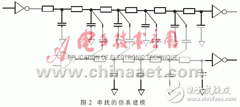
When several high-speed signals are striking and the distance between these lines is very close, the influence of crosstalk on the system cannot be ignored. The crosstalk between two parallel signal lines can be modeled using Figure 2. The signal on the "non-gate" output line in the figure will cause interference on the output line of the NAND gate. Conversely, the signal on the NAND gate output line will also cause interference on the NOT gate output line. It can be seen from the figure that if the distance between two parallel lines is smaller, the longer the parallel line parallel length, the greater the inductive coupling and capacitive coupling between the parallel lines, and the greater the crosstalk. From the perspective of reducing inductive coupling and capacitive coupling, the most effective way to eliminate crosstalk is to increase the spacing between parallel lines while minimizing the parallel length of parallel lines. It is of course also possible to change the dielectric property parameters of the printed board to reduce this coupling to reduce the crosstalk, but this may increase the cost of the board.

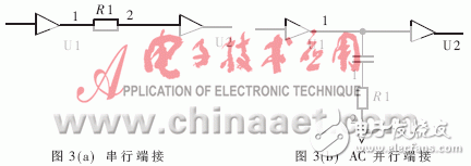
Sometimes, when the PCB board size is very demanding, it is not always possible to ensure sufficient space between the parallel lines. Therefore, it is necessary to appropriately change the wiring strategy, protect the important signal lines as much as possible, and rely on termination to greatly eliminate crosstalk. . The termination strategy may be different based on different routing topologies. There are three main methods: single-load network generally uses serial termination; daisy chain structure generally uses AC parallel termination; star wiring generally uses AC Parallel termination (as shown in Figure 3).

25*50mm Low Profile White Faceplate
included or excluded keystones for Keystones, or designed with PC board
fixtures and fittings provided
for Solid Cat 5 or Cat 6 cable
size is 25*50mm basing on UK type standard
Material as ABS, PC, PBT in UL94V-0 standards
Operation temperture -40~70 ℃
Could accept any combination of UONICRE Keystone Jack or RJ45 connectors
UK Face Plate,Outlet Face Plate,Wall Socket Face Plate,Face Plate Wall Socket
NINGBO UONICORE ELECTRONICS CO., LTD , https://www.uniconmelectronics.com