Vacuum systems have been widely used in electric power, petrochemical, medical and pharmaceutical, plastics, environmental protection, medical equipment and other industries. With the continuous expansion and deepening of vacuum applications, the requirements for vacuum technology are becoming higher and higher, for example, In the diamond coating device, since the deposition of the diamond film lasts for several tens of hours, the stability of the vacuum chamber vacuum has a great influence on the quality of the film formation, so maintaining the stability of the vacuum will become a key Technical problems; centrifugal pump in the vacuum pumping process and pump pumping process, the vacuum degree of the centrifugal pump inlet has become an important basis for the centrifugal pump start / stop, fault diagnosis. Only after the analog signal obtained by the pressure sensor is effectively A/D converted into a digital quantity, can be input into the MCU for processing, and communication with the PC and subsequent waveform display and analysis. The author proposes the combination of ADC0832 and pressure sensor (PTB710), and uses the program of the single-chip AT89S52 to control the conversion clock pulse method to detect the vacuum degree data.
1, A / D conversion circuit1.1, ADC0832 chip pin description Figure 1 is the pin diagram of ADC0832, where CS is the chip select terminal, active low; CH0, CH1 is two analog signal input; DI two analog input select input; DO For the analog-to-digital conversion result serial output; CLK is the serial clock input; VCC (REF) is the positive supply and reference input; GND is the power ground.
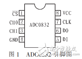
Table 1 shows the multiplexed addressing when the ADC0832 is operating, including single-ended multiplex mode and differential multiplex mode. Channel selection is performed by DI and DO data bit operations. When the bit data bit is "1", when "0", only single channel conversion is performed for CH0. When the 2-bit data is "1", "1", only CH1 is single-channel converted. When the 2-bit data is "0" and "0", CH0 is input as the positive input terminal IN+, and CH1 is input as the negative input terminal IN-.
Table 1 ADC0832 Multiplexing Mode
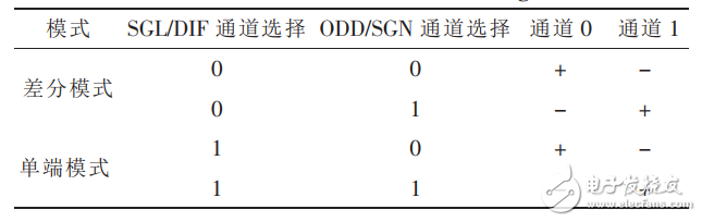
Figure 2 shows the interface circuit diagram of AT89s52 and ADC0832 in the schematic diagram used in this experiment. The chip select terminal is connected with the P2.3 port of the MCU, and the clock terminal is connected with the P2.2 port of the MCU. Since the selected I/O ports of the MCU are bidirectional, and the DI and DO terminals are not valid at the same time during operation, the two pins are connected in parallel and connected to the P2.1 port of the MCU for data communication. Figure 2 only shows the main control MCU, power-on reset, crystal oscillator and analog-to-digital conversion peripheral circuits. The default part includes power supply, detection and output port, triode switch and other logic conversion circuits. The design process takes into account the industrial site. Noise interference and other factors add optocoupler isolation at the input and output to enhance the anti-jamming performance of the circuit.
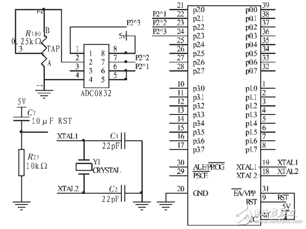
Figure 2 ADC0832 and AT89s52 interface circuit
Automotive Connectors,Automobile Pin Holder Connector,Industrial Automobile Connector,Waterproof Automotive Connector
Dongguan Yangyue Metal Technology Co., Ltd , https://www.yyconnector.com